JAJSVD5C August 2014 – October 2024 FDC1004
PRODUCTION DATA
- 1
- 1 特長
- 2 アプリケーション
- 3 概要
- 4 Pin Configuration and Functions
- 5 Specifications
- 6 Detailed Description
- 7 Applications and Implementation
- 8 Device and Documentation Support
- 9 Revision History
- 10Mechanical, Packaging, and Orderable Information
パッケージ・オプション
メカニカル・データ(パッケージ|ピン)
サーマルパッド・メカニカル・データ
- DSC|10
発注情報
4 Pin Configuration and Functions
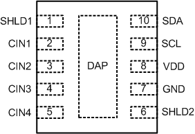
 Figure 4-1 WSON (DSC)10 PinsTOP
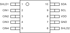
 Figure 4-2 VSSOP (DGS)10 PinsTOP
Table 4-1 Pin Functions
| PIN | TYPE(1) | DESCRIPTION | |
|---|---|---|---|
| NAME | NO. | ||
| SHLD1 | 1 | A | Capacitive Input Active AC Shielding. |
| CIN1 | 2 | A | Capacitive Input. The measured capacitance is connected between the CIN1 pin and GND. If not used, leave this pin as an open circuit. |
| CIN2 | 3 | A | Capacitive Input. The measured capacitance is connected between the CIN2 pin and GND. If not used, leave this pin as an open circuit. |
| CIN3 | 4 | A | Capacitive Input. The measured capacitance is connected between the CIN3 pin and GND. If not used, leave this pin as an open circuit. |
| CIN4 | 5 | A | Capacitive Input. The measured capacitance is connected between the CIN4 pin and GND. If not used, leave this pin as an open circuit. |
| SHLD2 | 6 | A | Capacitive Input Active AC Shielding. |
| GND | 7 | G | Ground |
| VDD | 8 | P | Power Supply Voltage. Decouple this pin to GND, using a low impedance capacitor, for example in combination with a 1μF tantalum and a 0.1μF multilayer ceramic. |
| SCL | 9 | I | Serial Interface Clock Input. Connects to the controller clock line. Requires pullup resistor if not already provided elsewhere in the system. |
| SDA | 10 | I/O | Serial Interface Bidirectional Data. Connects to the controller data line. Requires a pullup resistor if not provided elsewhere in the system. |
| DAP(2) | - | N/A | Connect to GND |
(1) P=Power, G=Ground, I=Input, O=Output, A=Analog,
I/O=Bidirectional Input/Output
(2) There is an internal electrical connection between the exposed
Die Attach Pad (DAP) and the GND pin of the device. Although the DAP can be left
floating, for best performance the DAP should be connected to the same potential
as the device's GND pin. Do not use the DAP as the primary ground for the
device. The device GND pin must always be connected to ground.