JAJSQA1C december 2015 – december 2020 HD3SS214
PRODUCTION DATA
- 1
- 1 特長
- 2 アプリケーション
- 3 概要
- 4 Revision History
- 5 Pin Configuration and Functions
-
6 Specifications
- 6.1 Absolute Maximum Ratings #GUID-AEF84F8B-5035-497D-BF42-BEE5DCF32E24/SLAS9018663 #GUID-AEF84F8B-5035-497D-BF42-BEE5DCF32E24/SLAS9012713
- 6.2 ESD Ratings
- 6.3 Recommended Operating Conditions
- 6.4 Thermal Information
- 6.5 Electrical Characteristics
- 6.6 Electrical Characteristics, Device Parameters
- 6.7 Timing Requirements
- 6.8 Typical Characteristics
- 7 Detailed Description
- 8 Application and Implementation
- 9 Power Supply Recommendations
- 10Layout
- 11Device and Documentation Support
- 12Mechanical, Packaging, and Orderable Information
8.2.3.2 Source Selection Interface
Two control pins on the HD3SS214 are responsible for selecting the incoming DP signal: Dx_SEL and AUX_SEL. Dx_SEL controls which high speed ports are selected. A low signal on Dx_SEL corresponds to Port A routed to Port C and a high signal corresponds to Port B routed to Port C. A slide switch is used to select the level for this signal. In an embedded application, this switch can be replaced by a GPIO signal from a microcontroller.
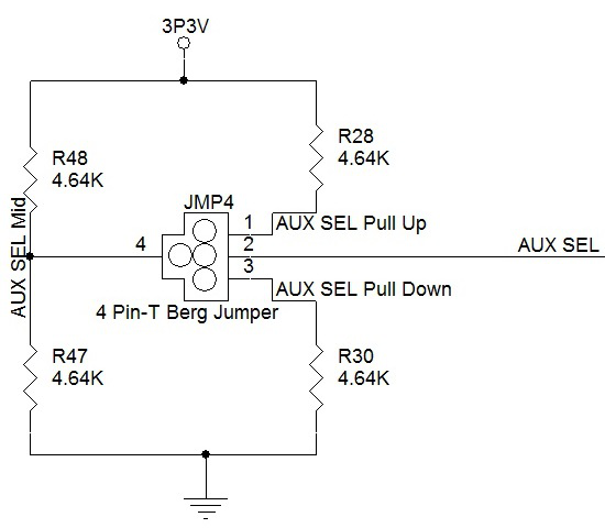
AUX channel is controlled by AUX_SEL. This pin configures the switch to route the incoming AUX signal to the outgoing AUX path, when AUX_SEL = 0 the AUXA channel will be routed to AUXC, when AUX_SEL = 1 the AUXB channel will be routed to AUXC. Figure 8-2 shows the selection circuitry.
 Figure 8-2 AUX_SEL Schematic