JAJSE69 December 2017 HD3SS3412A
PRODUCTION DATA.
- 1 特長
- 2 アプリケーション
- 3 概要
- 4 改訂履歴
- 5 概要(続き)
- 6 Pin Configuration and Functions
- 7 Specifications
- 8 Parameter Measurement Information
- 9 Detailed Description
- 10Application and Implementation
- 11Power Supply Recommendations
- 12Layout
- 13デバイスおよびドキュメントのサポート
- 14メカニカル、パッケージ、および注文情報
パッケージ・オプション
メカニカル・データ(パッケージ|ピン)
- RUA|42
サーマルパッド・メカニカル・データ
- RUA|42
発注情報
7 Specifications
7.1 Absolute Maximum Ratings
Over operating free-air temperature range (unless otherwise noted)(1)(2)| MIN | MAX | UNIT | ||
|---|---|---|---|---|
| Supply voltage (VDD) | Absolute minimum/maximum supply voltage | –0.5 | 4 | V |
| Voltage | Differential I/O | –0.5 | 4 | V |
| Control pin (SEL) | –0.5 | VDD + 0.5 | ||
| Storage temperature, Tstg | –65 | 150 | °C | |
(1) Stresses beyond those listed under Absolute Maximum Ratings may cause permanent damage to the device. These are stress ratings only and functional operation of the device at these or any conditions beyond those indicated under Recommended Operating Conditions is not implied. Exposure to absolute-maximum-rated conditions for extended periods may affect device reliability.
(2) All voltage values, except differential voltages, are with respect to network ground terminal.
7.2 ESD Ratings
| VALUE | UNIT | |||
|---|---|---|---|---|
| V(ESD) | Electrostatic discharge | Human-body model (HBM), per ANSI/ESDA/JEDEC JS-001(1) | ±4000 | V |
| Charged-device model (CDM), per JEDEC specification JESD22-C101(2) | ±1500 | |||
(1) JEDEC document JEP155 states that 500-V HBM allows safe manufacturing with a standard ESD control process.
(2) JEDEC document JEP157 states that 250-V CDM allows safe manufacturing with a standard ESD control process.
7.3 Recommended Operating Conditions
Typical values for all parameters are at VDD = 3.3 V and TA = 25°C. (Temperature limits are specified by design)| MIN | NOM | MAX | UNIT | |||
|---|---|---|---|---|---|---|
| VDD | Supply voltage | 3.0 | 3.3 | 3.6 | V | |
| VIH | Input high voltage (SEL pin) | 2.0 | VDD | V | ||
| VIL | Input low voltage (SEL pin) | –0.1 | 0.8 | V | ||
| VI/O_Diff | Differential voltage (differential pins) | Switch I/O diff voltage | 0 | 1.8 | VPP | |
| VI/O_CM | Common voltage (differential pins) | Switch I/O common-mode voltage | 0 | 2.0 | V | |
| TA | Operating free-air temperature | Ambient temperature | 0 | 70 | oC | |
7.4 Thermal Information
| THERMAL METRIC(1) | HD3SS3412A | UNIT | |
|---|---|---|---|
| RUA (WQFN) | |||
| 42 PINS | |||
| RθJA | Junction-to-ambient thermal resistance | 53.8 | °C/W |
| RθJC(top) | Junction-to-case (top) thermal resistance | 38.2 | °C/W |
| RθJB | Junction-to-board thermal resistance | 21.9 | °C/W |
| ψJT | Junction-to-top characterization parameter | 27.4 | °C/W |
| ψJB | Junction-to-board characterization parameter | 5.6 | °C/W |
| RθJC(bot) | Junction-to-case (bottom) thermal resistance | 27.3 | °C/W |
(1) For more information about traditional and new thermal metrics, see the Semiconductor and IC Package Thermal Metrics application report.
7.5 Electrical Characteristics
Over operating free-air temperature range (unless otherwise noted)| PARAMETER | TEST CONDITIONS | MIN | TYP | MAX | UNIT | |
|---|---|---|---|---|---|---|
| DEVICE PARAMETERS | ||||||
| IIH | Input High Voltage (SEL) | VDD = 3.6 V; VIN = VDD | 95 | µA | ||
| IIL | Input Low Voltage (SEL) | VDD = 3.6 V; VIN = GND | 1 | µA | ||
| ILK | Leakage Current (Differential I/O pins) | VDD = 3.6 V; VIN = 0 V; VOUT = 2 V (ILK On OPEN outputs) [Ports B and C] |
130 | µA | ||
| VDD = 3.6 V, VIN = 2 V; VOUT = 0 V (ILK On OPEN outputs) [Port A] |
4 | |||||
| IDD | Supply Current | VDD = 3.6 V; SEL = VDD/GND; Outputs Floating | 4.7 | 6 | mA | |
| CON | Outputs ON Capacitance | VIN = 0 V; Outputs Open; Switch ON | 1.5 | pF | ||
| COFF | Outputs OFF Capacitance | VIN = 0 V; Outputs Open, Switch OFF | 1 | pF | ||
| RON | Output ON resistance | VDD = 3.3 V; VCM = 0.5 V to 1.5 V ; IO = –8 mA | 5 | 8 | Ω | |
| ΔRON | ON-resistance match between channels | VDD = 3.3 V ; –0.35 V ≤ VIN ≤ 1.2 V; IO = –8 mA | 2 | Ω | ||
| ON-resistance match between pairs of the same channel | VDD = 3.3 V; –0.35 V ≤ VIN ≤ 1.2 V; IO = –8 mA | 0.7 | Ω | |||
| RFLAT_ON | ON-resistance flatness (RON(MAX) – RON(MAIN) |
VDD = 3.3 V; –0.35 V ≤ VIN ≤ 1.2 V | 1.15 | Ω | ||
| tPD | Switch propagation delay | Rsc and RLOAD = 50 Ω | 85 | ps | ||
| SEL-to-switch TON | Rsc and RLOAD = 50 Ω | 70 | 250 | ns | ||
| SEL-to-switch TOFF | 70 | 250 | ||||
| TSKEW_Inter | Inter-pair output skew (CH-CH) | Rsc and RLOAD = 50 Ω | 20 | ps | ||
| TSKEW_Intra | Intra-pair output skew (bit-bit) | Rsc and RLOAD = 50 Ω | 8 | ps | ||
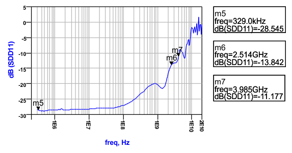
| RL | Differential return loss (VCM = 0 V) Also see Typical Characteristics |
f = 0.3 MHz | –28 | dB | ||
| f = 2500 MHz | –12 | |||||
| f = 4000 MHz | –11 | |||||
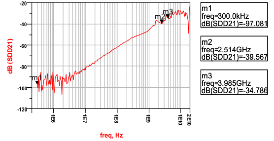
| XTALK | Differential Crosstalk(VCM = 0 V) Also see Typical Characteristics |
f = 0.3 MHz | –90 | dB | ||
| f = 2500 MHz | –39 | |||||
| f = 4000 MHz | –35 | |||||
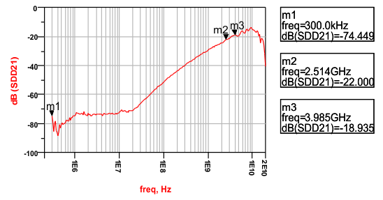
| OIRR | Differential Off-Isolation(VCM = 0 V) Also see Typical Characteristics |
f = 0.3 MHz | –75 | dB | ||
| f = 2500 MHz | –22 | |||||
| f = 4000 MHz | –19 | |||||
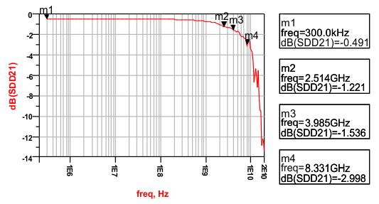
| IL | Differential Insertion Loss (VCM = 0 V) Also see Typical Characteristics |
f = 0.3 MHz | –0.5 | dB | ||
| f = 2500 MHz | –1.1 | |||||
| f = 4000 MHz | –1.5 | |||||
| BW | Bandwidth | At –3 dB | 8 | GHz | ||
7.6 Dissipation Ratings
| MIN | MAX | UNIT | ||
|---|---|---|---|---|
| PD | Power Dissipation | 15.5 | 21.6 | mW |
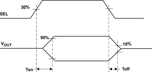 Figure 1. Switch ON and OFF Timing Diagram
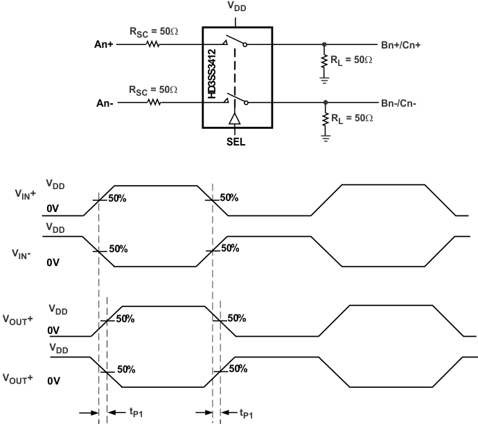
TSKEWInter = Difference between tPD for any two pairs of outputs
TSKEWIntra = Difference between tP1 and tP2 of same pair
Figure 2. Propagation Delay Timing Diagram and Test Setup
7.7 Typical Characteristics
