SLLSEC4B June 2013 – August 2016 HVDA551-Q1 , HVDA553-Q1
PRODUCTION DATA.
- 1 Features
- 2 Applications
- 3 Description
- 4 Revision History
- 5 Pin Configuration and Functions
- 6 Specifications
- 7 Parameter Measurement Information
- 8 Detailed Description
- 9 Application and Implementation
- 10Power Supply Recommendations
- 11Layout
- 12Device and Documentation Support
- 13Mechanical, Packaging, and Orderable Information
7 Parameter Measurement Information
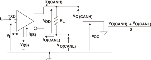
 Figure 2. Driver Voltage, Current, and Test Definition
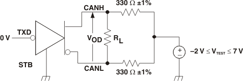
 Figure 3. Driver VOD Test Circuit

A. The input pulse is supplied by a generator having the following characteristics: PRR ≤ 125 kHz, 50% duty cycle, tr ≤ 6 ns, tf ≤ 6 ns, ZO = 50 Ω.
B. CL includes instrumentation and fixture capacitance within ±20%.
C. For HVDA553 device versions, VIO = VCC.
Figure 4. Driver Test Circuit and Voltage Waveforms
 Figure 5. Receiver Voltage and Current Definitions

A. The input pulse is supplied by a generator having the following characteristics: PRR ≤ 125 kHz, 50% duty cycle, tr ≤ 6 ns, tf ≤ 6 ns, ZO = 50 Ω.
B. CL includes instrumentation and fixture capacitance within ±20%.
C. For HVDA553 device versions VIO = VCC.
Figure 6. Receiver Test Circuit and Voltage Waveforms
Table 1. Differential Input Voltage Threshold Test
| INPUT | OUTPUT | |||
|---|---|---|---|---|
| VCANH | VCANL | |VID| | R | |
| –11.1 V | –12 V | 900 mV | L | VOL |
| 12 V | 11.1 V | 900 mV | L | |
| –6 V | –12 V | 6 V | L | |
| 12 V | 6 V | 6 V | L | |
| –11.5 V | –12 V | 500 mV | H | VOH |
| 12 V | 11.5 V | 500 mV | H | |
| –12 V | –6 V | 6 V | H | |
| 6 V | 12 V | 6 V | H | |
| Open | Open | X | H | |

A. CL = 100 pF includes instrumentation and fixture capacitance within ±20%.
B. All VI input pulses are from 0 V to VIO and supplied by a generator having the following characteristics: tr or tf ≤ 6 ns. Pulse repetition rate (PRR) = 25 kHz, 50% duty cycle.
C. For HVDA553 device versions, VIO = VCC.
Figure 7. tEN Test Circuit and Waveforms

A. All VI input pulses are from 0 V to VIO and supplied by a generator having the following characteristics: tr or tf ≤ 6 ns. Pulse repetition rate (PRR) = 125 kHz, 50% duty cycle.
Figure 8. Common-Mode Output Voltage Test and Waveforms

A. CL = 100 pF includes instrumentation and fixture capacitance within ±20%.
B. All VI input pulses are from 0 V to VIO and supplied by a generator having the following characteristics: tr or tf ≤ 6 ns. Pulse repetition rate (PRR) = 125 kHz, 50% duty cycle.
C. For HVDA553 device versions, VIO = VCC.
Figure 9. tPROP(LOOP) Test Circuit and Waveform

A. CL = 100 pF includes instrumentation and fixture capacitance within ±20%.
B. All VI input pulses are from 0 V to VIO and supplied by a generator having the following characteristics: tr or tf ≤ 6 ns. Pulse repetition rate (PRR) = 500 Hz, 50% duty cycle.
C. For HVDA553 device versions, VIO = VCC.
Figure 10. TXD Dominant Time-Out Test Circuit and Waveforms

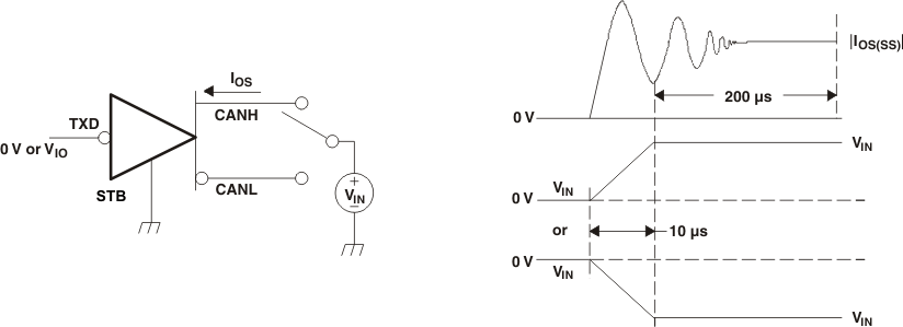
A. For HVDA553 device versions VIO = VCC.
Figure 11. Driver Short-Circuit Current Test and Waveforms

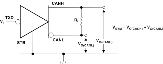
A. All VI input pulses are from 0 V to VIO and supplied by a generator having the following characteristics: tr and tf ≤ 6 ns, pulse repetition rate (PRR) = 250 kHz, 50% duty cycle.
Figure 12. Driver Output Symmetry Test Circuit