SBOS501F January 2010 – February 2015 INA128-HT , INA129-HT
PRODUCTION DATA.
- 1 Features
- 2 Applications
- 3 Description
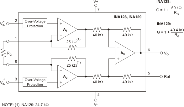
- 4 Simplified Schematic
- 5 Revision History
- 6 Pin Configuration and Functions
- 7 Specifications
- 8 Detailed Description
- 9 Application and Implementation
- 10Power Supply Recommendations
- 11Layout
- 12Device and Documentation Support
- 13Mechanical, Packaging, and Orderable Information
パッケージ・オプション
メカニカル・データ(パッケージ|ピン)
サーマルパッド・メカニカル・データ
発注情報
1 Features
- Low Offset Voltage: 25 uV Typical
- Low Input Bias Current: 50 nA Typical (1)
- High CMR: 95 dB Typical(1)
- Inputs Protected to ±40 V
- Wide Supply Range: ±2.25 V to ±18 V
- Low Quiescent Current: 2 mA Typical(1)
2 Applications
- Bridge Amplifiers
- Thermocouple Amplifiers
- RTD Sensor Amplifiers
- Medical Instrumentation
- Data Acquisition
- Supports Extreme Temperature Applications:
- Controlled Baseline
- One Assembly/Test Site
- One Fabrication Site
- Available in Extreme Temperature Ranges
(–55°C to 210°C) (1) - Extended Product Life Cycle
- Extended Product-Change Notification
- Product Traceability
3 Description
The INA128-HT and INA129-HT are low-power, general-purpose instrumentation amplifiers offering excellent accuracy. The versatile three-operational-amplifier design and small size make them ideal for a wide range of applications. Current-feedback input circuitry provides wide bandwidth even at high gain. A single external resistor sets any gain from 1 to 10000. The INA128-HT provides an industry-standard gain equation; the INA129-HT gain equation is compatible with the AD620.
The INA128-HT and INA129-HT are laser trimmed for very low offset voltage (25 μV Typ) and high common-mode rejection (93 dB at G ≥ 100). These devices operate with power supplies as low as ±2.25 V, and quiescent current of 2 mA, typically. Internal input protection can withstand up to ±40 V without damage.
Texas Instruments' high-temperature products use highly optimized silicon (die) solutions with design and process enhancements to maximize performance over extended temperatures.
The INA129-HT is available in 8-pin ceramic DIP and 8-pin ceramic surface-mount packages, specified for the –55°C to 210°C temperature range. The INA128-HT is available in an 8-pin SOIC-8 surface-mount package, specified for the –55°C to 175°C temperature range.
Device Information(1)
| PART NUMBER | PACKAGE | BODY SIZE (NOM) |
|---|---|---|
| INA128-HT | SOIC (8) | 4.90 mm × 3.91 mm |
| INA129-HT | CFP (8) | 6.90 mm × 5.65 mm |
| CDIP SB (8) | 11.81 mm × 7.49 mm |
- For all available packages, see the orderable addendum at the end of the data sheet.
4 Simplified Schematic