JAJSCW1C July 2016 – December 2016 INA260
PRODUCTION DATA.
- 1 特長
- 2 アプリケーション
- 3 概要
- 4 改訂履歴
- 5 Related Products
- 6 Pin Configuration and Functions
- 7 Specifications
-
8 Detailed Description
- 8.1 Overview
- 8.2 Functional Block Diagram
- 8.3 Feature Description
- 8.4 Device Functional Modes
- 8.5 Programming
- 8.6
Register Maps
- 8.6.1 Configuration Register (00h) (Read/Write)
- 8.6.2 Current Register (01h) (Read-Only)
- 8.6.3 Bus Voltage Register (02h) (Read-Only)
- 8.6.4 Power Register (03h) (Read-Only)
- 8.6.5 Mask/Enable Register (06h) (Read/Write)
- 8.6.6 Alert Limit Register (07h) (Read/Write)
- 8.6.7 Manufacturer ID Register (FEh) (Read-Only)
- 8.6.8 Die ID Register (FFh) (Read-Only)
- 9 Application and Implementation
- 10Power Supply Recommendations
- 11Layout
- 12デバイスおよびドキュメントのサポート
- 13メカニカル、パッケージ、および注文情報
9 Application and Implementation
NOTE
Information in the following applications sections is not part of the TI component specification, and TI does not warrant its accuracy or completeness. TI’s customers are responsible for determining suitability of components for their purposes. Validate and test the design implementation to confirm system functionality.
9.1 Application Information
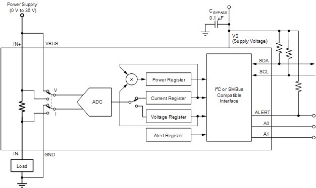
The INA260 is a current shunt and power monitor with an I2C-compatible interface. The device monitors both a shunt current and bus supply voltage. The internally calibrated integrated current sense resistor combined with an internal multiplier, enable direct readouts of current in amperes and power in watts.
9.2 Typical Application
 Figure 30. Typical Circuit Configuration, INA260
9.2.1 Design Requirements
The INA260 measures current and the bus supply voltage and calculates power. It comes with alert capability where the ALERT pin can be programmed to respond to a user-defined event or to a conversion ready notification. This design illustrates the ability of the ALERT pin to respond to a set threshold.
9.2.2 Detailed Design Procedure
The ALERT pin can be configured to respond to one of the five alert functions described in the ALERT Pin section. The ALERT pin must be pulled up to the VS pin voltage through an external pullup resistor. The configuration register is set based on the required conversion time and averaging. The Mask/Enable Register is set to identify the required alert function and the Alert Limit Register is set to the limit value used for comparison.
9.2.3 Application Curves
Figure 32 shows the ALERT pin response to a bus over voltage limit of 5.5 V for a conversion time (tCT) of 1.1 ms and averaging set to 1. Figure 31 shows the response for the same limit but with the conversion time reduced to 140 µs. For the scope shots shown in these figures, persistence was enabled on the ALERT channel. This shows how the ALERT response time can vary depending on when the fault condition occurs relative to the internal ADC clock of the INA260. For fault conditions that are just exceeding the limit threshold the response time for the ALERT pin can vary from 1 to 2 conversion cycles. As mentioned, the variation is due to the timing on when the fault event occurs relative to the start time of the internal ADC conversion cycle. For fault events that greatly exceed the limit threshold it is possible for the alert to respond in less than one conversion cycle. This is because it takes fewer samples for the average to exceed the limit threshold value.
Table 17. Configuration Register (00h) Settings for Figure 31 (Value = 6006h)
| BIT # | 15 | 14 | 13 | 12 | 11 | 10 | 9 | 8 | 7 | 6 | 5 | 4 | 3 | 2 | 1 | 0 |
|---|---|---|---|---|---|---|---|---|---|---|---|---|---|---|---|---|
| BIT NAME |
RST | — | — | — | AVG2 | AVG1 | AVG0 | VBUSCT2 | VBUSCT1 | VBUSCT0 | ISHCT2 | ISHCT1 | ISHCT0 | MODE3 | MODE2 | MODE1 |
| POR VALUE | 0 | 1 | 1 | 0 | 0 | 0 | 0 | 0 | 0 | 0 | 0 | 0 | 0 | 1 | 1 | 0 |
Table 18. Configuration Register (00h) Settings for Figure 32 (Value = 6126h)
| BIT # | 15 | 14 | 13 | 12 | 11 | 10 | 9 | 8 | 7 | 6 | 5 | 4 | 3 | 2 | 1 | 0 |
|---|---|---|---|---|---|---|---|---|---|---|---|---|---|---|---|---|
| BIT NAME |
RST | — | — | — | AVG2 | AVG1 | AVG0 | VBUSCT2 | VBUSCT1 | VBUSCT0 | ISHCT2 | ISHCT1 | ISHCT0 | MODE3 | MODE2 | MODE1 |
| POR VALUE | 0 | 1 | 1 | 0 | 0 | 0 | 0 | 1 | 0 | 0 | 1 | 0 | 0 | 1 | 1 | 0 |

