JAJSEI7E February   2007  – January 2018 INA270 , INA271

PRODUCTION DATA.  

  1. 特長
  2. アプリケーション
  3. 概要
    1.     Device Images
      1.      概略回路図
  4. 改訂履歴
  5. Device Comparison Table
  6. Pin Configuration and Functions
    1.     Pin Functions
  7. Specifications
    1. 7.1 Absolute Maximum Ratings
    2. 7.2 ESD Ratings
    3. 7.3 Recommended Operating Conditions
    4. 7.4 Thermal Information
    5. 7.5 Electrical Characteristics
    6. 7.6 Typical Characteristics
  8. Detailed Description
    1. 8.1 Overview
    2. 8.2 Functional Block Diagram
    3. 8.3 Feature Description
      1. 8.3.1 Basic Connection
      2. 8.3.2 Selecting RS
      3. 8.3.3 Transient Protection
    4. 8.4 Device Functional Modes
      1. 8.4.1 First- or Second-Order Filtering
      2. 8.4.2 Accuracy Variations as a Result of VSENSE and Common-Mode Voltage
        1. 8.4.2.1 Normal Case 1: VSENSE ≥ 20 mV, VCM ≥ VS
        2. 8.4.2.2 Normal Case 2: VSENSE ≥ 20 mV, VCM < VS
        3. 8.4.2.3 Low VSENSE Case 1: VSENSE < 20 mV, –16 V ≤ VCM < 0; and Low VSENSE Case 3: VSENSE < 20 mV, VS < VCM ≤ 80 V
        4. 8.4.2.4 Low VSENSE Case 2: VSENSE < 20 mV, 0 V ≤ VCM ≤ VS
  9. Application and Implementation
    1. 9.1 Application Information
    2. 9.2 Typical Application
      1. 9.2.1 Design Requirements
      2. 9.2.2 Detailed Design Procedure
      3. 9.2.3 Application Curves
  10. 10Power Supply Recommendations
    1. 10.1 Shutdown
  11. 11Layout
    1. 11.1 Layout Guidelines
      1. 11.1.1 RFI and EMI
    2. 11.2 Layout Example
  12. 12デバイスおよびドキュメントのサポート
    1. 12.1 ドキュメントのサポート
      1. 12.1.1 関連資料
    2. 12.2 関連リンク
    3. 12.3 コミュニティ・リソース
    4. 12.4 商標
    5. 12.5 静電気放電に関する注意事項
    6. 12.6 Glossary
  13. 13メカニカル、パッケージ、および注文情報

パッケージ・オプション

メカニカル・データ(パッケージ|ピン)
サーマルパッド・メカニカル・データ
発注情報

Application Curves

Figure 20 shows the output waveform without filtering. The output signal tracks the input signal with a large ripple. If this current is sampled by an ADC, many samples must be taken to average the current digitally. This process takes additional time to sample and average and is very time consuming, thus is unwanted for this application.

Figure 21 shows the output waveform with filtering. The output signal is filtered and the average can easily be measured with a small ripple. If this current is sampled by an ADC, only a few samples must be taken to average. Digital averaging is now not required and the time required is significantly reduced.

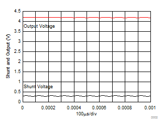
INA270 INA271 D020_SBOS381.gif
Figure 20. Without Filtering
INA270 INA271 D021_SBOS381.gif
Figure 21. With Filtering