-
INA28x High-Accuracy, Wide Common-Mode Range, Bidirectional Current Shunt Monitors, Zero-Drift Series
- 1 Features
- 2 Applications
- 3 Description
- 4 Revision History
- 5 Pin Configuration and Functions
- 6 Specifications
- 7 Detailed Description
- 8 Applications and Implementation
- 9 Power Supply Recommendations
- 10Layout
- 11Device and Documentation Support
- 12Mechanical, Packaging, and Orderable Information
- IMPORTANT NOTICE
パッケージ・オプション
メカニカル・データ(パッケージ|ピン)
サーマルパッド・メカニカル・データ
発注情報
INA28x High-Accuracy, Wide Common-Mode Range, Bidirectional Current Shunt Monitors, Zero-Drift Series
1 Features
2 Applications
- Telecom Equipment
- Automotive
- Power Management
- Solar Inverters
3 Description
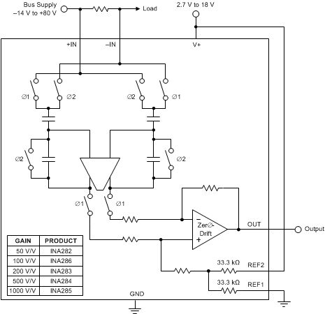
The INA28x family includes the INA282, INA283, INA284, INA285, and INA286 devices. These devices are voltage output current shunt monitors that can sense drops across shunts at common-mode voltages from –14 V to +80 V, independent of the supply voltage. The low offset of the zero-drift architecture enables current sensing with maximum drops across the shunt as low as 10 mV full-scale.
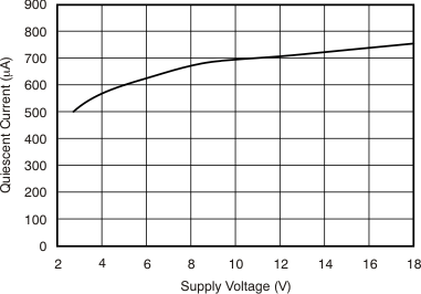
These current sense amplifiers operate from a single +2.7-V to +18-V supply, drawing a maximum of 900 μA of supply current. These devices are specified over the extended operating temperature range of –40°C to +125°C, and offered in SOIC-8 and VSSOP-8 packages.
Device Information(1)
| ORDER NUMBER | PACKAGE | BODY SIZE (NOM) |
|---|---|---|
| INA28x | SOIC (8) | 4.90 mm x 3.91 mm |
| VSSOP (8) | 3.00 mm x 3.00 mm |
- For all available packages, see the package option addendum at the end of the datasheet.
4 Revision History
Changes from B Revision (September 2012) to C Revision
- Added DGK (VSSOP) package to data sheetGo
- Changed front page diagramGo
- Added ESD Ratings and Recommended Operating Conditions tables, and Feature Description, Application and Implementation, Power Supply Recommendations ,Layout , Device and Documentation Support , and Mechanical, Packaging, and Orderable Information sectionsGo
- Deleted Machine Model ESD ratingGo
- Changed HBM ESD rating from ±3000 V to ±2000 VGo
- Added RVRR as symbol for reference voltage rejection ratio Go
- Changed order of figures in Typical Characteristics sectionGo
- Changed Figure 16Go
- Changed VDRIVE condition in Figure 19 and Figure 20Go
- Added functional block diagramGo
- Changed Figure 32 and Figure 33Go
- Changed Figure 34 and Figure 35Go
- Changed Figure 36 and Figure 37Go
- Changed Figure 38Go
- Changed Reference Common-Mode Rejection to Reference Voltage Rejection RatioGo
- Changed RCMR to RVRR in Table 1 and Table 2Go
- Changed Figure 39Go
- Changed Figure 40Go
- Changed Figure 42Go
Changes from A Revision (July 2010) to B Revision
- Changed devices from product preview to production data.Go
5 Pin Configuration and Functions

Pin Descriptions
| PIN | I/O | DESCRIPTION | |
|---|---|---|---|
| NO. | NAME | ||
| 1 | –IN | Analog input | Connect this pin to load side of shunt resistor. |
| 2 | GND | Analog | Ground |
| 3 | REF2 | Analog input | Reference voltage, 0 V to V+. See Reference Pin Connection Options section for connection options. |
| 4 | NC | — | This pin is not internally connected. Either float or connect this pin to GND. |
| 5 | OUT | Analog output | Output voltage |
| 6 | V+ | Analog | Power supply, 2.7 V to 18 V |
| 7 | REF1 | Analog input | Reference voltage, 0 V to V+. See Reference Pin Connection Options section for connection options. |
| 8 | +IN | Analog input | Connect this pin to supply side of shunt resistor. |
6 Specifications
6.1 Absolute Maximum Ratings
Over operating free-air temperature range (unless otherwise noted)(1)| MIN | MAX | UNIT | ||
|---|---|---|---|---|
| Supply voltage, V+ | 18 | V | ||
| Analog inputs, V+IN, V–IN(2) | Differential (V+IN) – (V–IN)(3) | –5 | +5 | V |
| Common-mode | –14 | +80 | V | |
| REF1, REF2, OUT | GND – 0.3 | (V+) + 0.3 | V | |
| Input current into any pin | 5 | mA | ||
| Junction temperature | 150 | °C | ||
| Storage temperature range, Tstg | –65 | +150 | °C | |
6.2 ESD Ratings
| VALUE | UNIT | |||
|---|---|---|---|---|
| V(ESD) | Electrostatic discharge | Human-body model (HBM), per ANSI/ESDA/JEDEC JS-001(1) | ±2000 | V |
| Charged-device model (CDM), per JEDEC specification JESD22-C101(2) | ±1000 | |||
6.3 Recommended Operating Conditions
over operating free-air temperature range (unless otherwise noted)| MIN | NOM | MAX | UNIT | ||
|---|---|---|---|---|---|
| VCM | Common-mode input voltage | 12 | V | ||
| V+ | Operating supply voltage | 5 | V | ||
| TA | Operating free-air temperature | –40 | +125 | °C | |
6.4 Thermal Information
| THERMAL METRIC(1) | INA28x | UNIT | ||
|---|---|---|---|---|
| D (SOIC) | DGK (VSSOP) | |||
| 8 PINS | 8 PINS | |||
| RθJA | Junction-to-ambient thermal resistance | 134.9 | 164.1 | °C/W |
| RθJC(top) | Junction-to-case (top) thermal resistance | 72.9 | 56.4 | °C/W |
| RθJB | Junction-to-board thermal resistance | 61.3 | 85.0 | °C/W |
| ψJT | Junction-to-top characterization parameter | 18.9 | 6.5 | °C/W |
| ψJB | Junction-to-board characterization parameter | 54.3 | 83.3 | °C/W |
| RθJC(bot) | Junction-to-case (bottom) thermal resistance | n/a | n/a | °C/W |
6.5 Electrical Characteristics
At TA = 25°C, V+ = 5 V, V+IN = 12 V, VREF1 = VREF2 = 2.048 V referenced to GND, and VSENSE = V+IN – V–IN (unless otherwise noted)| PARAMETER | TEST CONDITIONS | MIN | TYP | MAX | UNIT | ||
|---|---|---|---|---|---|---|---|
| INPUT | |||||||
| VOS | Offset voltage, RTI(1) | VSENSE = 0 mV | ±20 | ±70 | µV | ||
| dVOS/dT | vs temperature | VSENSE = 0 mV, TA = –40°C to +125°C |
±0.3 | ±1.5 | µV/°C | ||
| PSRR | vs power supply | V+ = +2.7 V to +18 V, VSENSE = 0 mV |
3 | μV/V | |||
| VCM | Common-mode input range | TA = –40°C to +125°C | –14 | +80 | V | ||
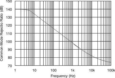
| CMRR | Common-mode rejection ratio | V+IN = –14 V to +80 V, VSENSE = 0 mV, TA = –40°C to +125°C |
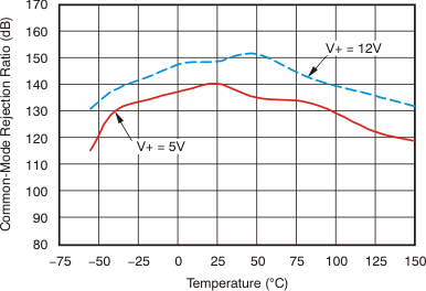
120 | 140 | dB | ||
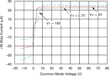
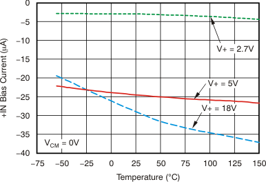
| IB | Input bias current per pin(2) | VSENSE = 0 mV | 25 | µA | |||
| IOS | Input offset current | VSENSE = 0 mV | 1 | µA | |||
| Differential input impedance | 6 | kΩ | |||||
| REFERENCE INPUTS | |||||||
| Reference input gain | 1 | V/V | |||||
| Reference input voltage range(3) | 0 | VGND + 9 | V | ||||
| Divider accuracy(4) | ±0.2% | ±0.5% | |||||
| RVRR | Reference voltage rejection ratio (VREF1 = VREF2 = 40 mV to 9 V, V+ = 18 V) |
INA282 | ±25 | ±75 | µV/V | ||
| TA = –40°C to +125°C | 0.055 | µV/V/°C | |||||
| INA283 | ±13 | ±30 | µV/V | ||||
| TA = –40°C to +125°C | 0.040 | µV/V/°C | |||||
| INA284 | ±6 | ±25 | µV/V | ||||
| TA = –40°C to +125°C | 0.015 | µV/V/°C | |||||
| INA285 | ±4 | ±10 | µV/V | ||||
| TA = –40°C to +125°C | 0.010 | µV/V/°C | |||||
| INA286 | ±17 | ±45 | µV/V | ||||
| TA = –40°C to +125°C | 0.040 | µV/V/°C | |||||
| GAIN(5) (GND + 0.5 V ≤ VOUT ≤ (V+) – 0.5 V; VREF1 = VREF2 = (V+) / 2 for all devices) | |||||||
| G | Gain | INA282, V+ = 5 V | 50 | V/V | |||
| INA283, V+ = 5 V | 200 | V/V | |||||
| INA284, V+ = 12 V | 500 | V/V | |||||
| INA285, V+ = 12 V | 1000 | V/V | |||||
| INA286, V+ = 5 V | 100 | V/V | |||||
| Gain error | INA282, INA283, INA286 | ±0.4% | ±1.4% | ||||
| INA284, INA285 | ±0.4% | ±1.6% | |||||
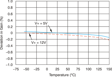
| TA = –40°C to +125°C | 0.0008 | 0.005 | %/°C | ||||
| OUTPUT | |||||||
| Nonlinearity error | ±0.01% | ||||||
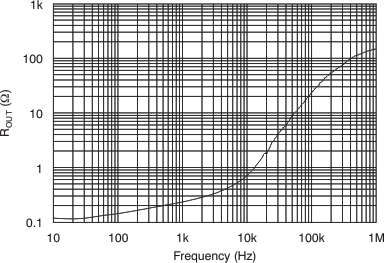
| Output impedance | 1.5 | Ω | |||||
| Maximum capacitive load | No sustained oscillation | 1 | nF | ||||
| VOLTAGE OUTPUT(6) | |||||||
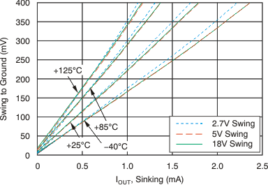
| Swing to V+ power-supply rail | V+ = 5 V, RLOAD = 10 kΩ to GND, TA = –40°C to +125°C |
(V+) – 0.17 | (V+) – 0.4 | V | |||
| Swing to GND | RLOAD = 10 kΩ to GND, TA = –40°C to +125°C |
GND + 0.015 | GND + 0.04 | V | |||
| FREQUENCY RESPONSE | |||||||
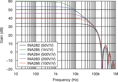
| BW | Effective bandwidth(7) | INA282 | 10 | kHz | |||
| INA283 | 10 | kHz | |||||
| INA284 | 4 | kHz | |||||
| INA285 | 2 | kHz | |||||
| INA286 | 10 | kHz | |||||
| NOISE, RTI(1) | |||||||
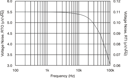
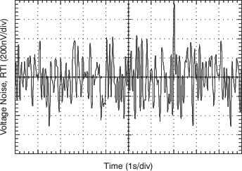
| Voltage noise density | 1 kHz | 110 | nV/√Hz | ||||
| POWER SUPPLY | |||||||
| VS | Specified voltage range | TA = –40°C to +125°C | 2.7 | 18 | V | ||
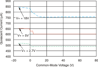
| IQ | Quiescent current | 600 | 900 | µA | |||
6.6 Typical Characteristics
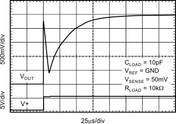
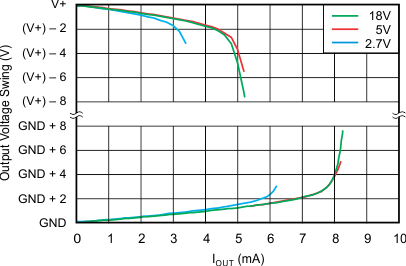
At TA = 25°C, V+ = 5 V, V+IN = 12 V, VREF1 = VREF2 = 2.048 V referenced to GND, and VSENSE = V+IN – V–IN (unless otherwise noted)