SBOS485C November 2009 – May 2015 INA282 , INA283 , INA284 , INA285 , INA286
PRODUCTION DATA.
- 1 Features
- 2 Applications
- 3 Description
- 4 Revision History
- 5 Pin Configuration and Functions
- 6 Specifications
- 7 Detailed Description
- 8 Applications and Implementation
- 9 Power Supply Recommendations
- 10Layout
- 11Device and Documentation Support
- 12Mechanical, Packaging, and Orderable Information
パッケージ・オプション
メカニカル・データ(パッケージ|ピン)
サーマルパッド・メカニカル・データ
発注情報
7 Detailed Description
7.1 Overview
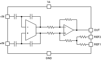
The INA28x family of voltage output current-sensing amplifiers are specifically designed to accurately measure voltages developed across current-sensing resistors on common-mode voltages that far exceed the supply voltage powering the devices. This family features a common-mode range that extends 14 V below the negative supply rail, as well as up to 80 V, allowing for either low-side or high-side current sensing while the device is powered from supply voltages as low as 2.7 V.
The zero-drift topology enables high-precision measurements with maximum input offset voltages as low as 70 µV with a maximum temperature contribution of 1.5 µV/°C over the full temperature range of –40°C to +125°C.
7.3 Feature Description
7.3.1 Selecting RS
The zero-drift offset performance of the INA28x family offers several benefits. Most often, the primary advantage of the low offset characteristic enables lower full-scale drops across the shunt. For example, nonzero-drift, current-shunt monitors typically require a full-scale range of 100 mV. The INA28x family gives equivalent accuracy at a full-scale range on the order of 10 mV. This accuracy reduces shunt dissipation by an order of magnitude, with many additional benefits. Alternatively, applications that must measure current over a wide dynamic range can take advantage of the low offset on the low end of the measurement. Most often, these applications can use the lower gains of the INA282, INA286, or INA283 to accommodate larger shunt drops on the upper end of the scale. For instance, an INA282 operating on a 3.3-V supply can easily handle a full-scale shunt drop of 55 mV, with only 70 μV of offset.
7.3.2 Effective Bandwidth
The extremely high dc CMRR of the INA28x family results from the switched-capacitor input structure. Because of this architecture, the INA28x exhibits discrete time-system behaviors, as illustrated in the Gain vs Frequency curve of Figure 1 and the Step Response curves of Figure 21 through Figure 28. The response to a step input depends in part on the phase of the internal INA28x clock when the input step occurs. It is possible to overload the input amplifier with a rapid change in input common-mode voltage (see Figure 4). Errors as a result of common-mode voltage steps or overload situations typically disappear within 15 μs after the disturbance is removed.
7.3.3 Transient Protection
The –14-V to +80-V common-mode range of the INA28x family is ideal for withstanding automotive fault conditions that range from 12-V battery reversal up to 80-V transients; no additional protective components are needed up to those levels. In the event that the INA28x family is exposed to transients on the inputs in excess of its ratings, then external transient absorption with semiconductor transient absorbers (Zener diodes or transorbs) are required. Use of metal-oxide varistors (MOVs) or voltage-dependent resistors (VDRs) is not recommended except when they are used in addition to a semiconductor transient absorber. Select a transient absorber that does not allow the INA28x family to be exposed to transients greater than 80 V (that is, allow for transient absorber tolerance, as well as additional voltage as a result of transient absorber dynamic impedance). Despite the use of internal zener-type electrostatic discharge (ESD) protection, the INA28x family does not lend itself to using external resistors in series with the inputs without degrading gain accuracy.
7.4 Device Functional Modes
7.4.1 Reference Pin Connection Options
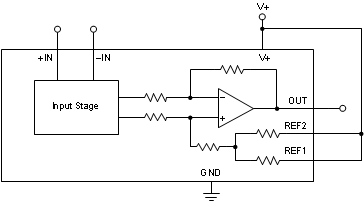
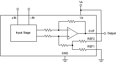
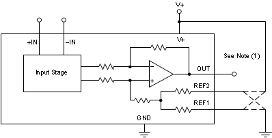
Figure 32 illustrates a test circuit for reference-divider accuracy. The output of the INA28x family can be connected for unidirectional or bidirectional operation. Do not connect the REF1 pin or the REF2 pin to any voltage source lower than GND or higher than V+. The effective reference voltage (REF1 + REF2) / 2 must be 9 V or less. This parameter means that the V+ reference output connection shown in Figure 34 is not allowed for a V+ value greater than 9 V. However, the split-supply reference connection shown in Figure 36 is allowed for all values of V+ up to 18 V.
7.4.1.1 Unidirectional Operation
Unidirectional operation allows the INA28x family to measure currents through a resistive shunt in one direction. In the case of unidirectional operation, set the output at the negative rail (near ground, and the most common connection) or at the positive rail (near V+) when the differential input is 0 V. The output moves to the opposite rail when a correct polarity differential input voltage is applied.
The required polarity of the differential input depends on the output voltage setting. If the output is set at the positive rail, the input polarity must be negative to move the output down. If the output is set at ground, the polarity is positive to move the output up.
The following sections describe how to configure the output for unidirectional operation.
7.4.1.1.1 Ground Referenced Output
When using the INA28x family in ground referenced output mode, both reference inputs are connected to ground; this configuration takes the output to the negative rail when there is 0 V differential at the input (as Figure 33 shows).
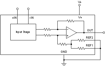 Figure 33. Ground Referenced Output
7.4.1.1.2 V+ Referenced Output
V+ referenced output mode is set when both reference pins are connected to the positive supply. This mode is typically used when a diagnostic scheme requires detection of the amplifier and the wiring before power is applied to the load (as shown in Figure 34).
7.4.1.2 Bidirectional Operation
Bidirectional operation allows the INA28x family to measure currents through a resistive shunt in two directions. In this case, the output can be set anywhere within the limits of what the reference inputs allow (that is, between 0 V to 9 V, but never to exceed the supply voltage). Typically, the reference inputs are set at half-scale for equal range in both directions. In some cases, however, the reference inputs are set at a voltage other than half-scale when the bidirectional current is nonsymmetrical.
The quiescent output voltage is set by applying voltage or voltages to the reference inputs. REF1 and REF2 are connected to internal resistors that connect to an internal offset node. There is no operational difference between the pins.
7.4.1.2.1 External Reference Output
Connecting both pins together and to a reference produces an output at the reference voltage when there is no differential input; this configuration is illustrated in Figure 35. The output moves down from the reference voltage when the input is negative relative to the –IN pin and up when the input is positive relative to the –IN pin. Note that this technique is the most accurate way to bias the output to a precise voltage.
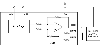 Figure 35. External Reference Output
7.4.1.2.2 Splitting The Supply
By connecting one reference pin to V+ and the other to the ground pin, the output is set at half of the supply when there is no differential input, as shown in Figure 36. This method creates a midscale offset that is ratiometric to the supply voltage; thus, if the supply increases or decreases, the output remains at half the supply.
7.4.1.2.3 Splitting an External Reference
In this case, an external reference is divided by two with an accuracy of approximately 0.5% by connecting one REF pin to ground and the other REF pin to the reference (as Figure 37 illustrates).
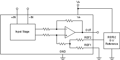 Figure 37. Split Reference Output
7.4.2 Shutdown
While the INA28x family does not provide a shutdown pin, the quiescent current of 600 μA enables the device to be powered from the output of a logic gate. Take the gate low to shut down the INA28x family devices.
7.4.3 Extended Negative Common-Mode Range
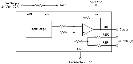
Using a negative power supply can extend the common-mode range 14 V more negative than the supply used. For instance, a –10-V supply allows up to a –24-V negative common-mode. Remember to keep the total voltage between the GND pin and V+ pin to less than 18 V. The positive common-mode decreases by the same amount.
The reference input simplifies this type of operation because the output quiescent bias point is always based on the reference connections. Figure 38 shows a circuit configuration for common-mode ranges from –24 V to +70 V.
7.4.4 Calculating Total Error
The electrical specifications for the INA28x family of devices include the typical individual errors terms such as gain error, offset error, and nonlinearity error. Total error including all of these individual error components is not specified in the Electrical Characteristics table. In order to accurately calculate the expected error of the device, the operating conditions of the device must first be known. Some current shunt monitors specify a total error in the product data sheet. However, this total error term is accurate under only one particular set of operating conditions. Specifying the total error at this one point has little practical value because any deviation from these specific operating conditions no longer yields the same total error value. This section discusses the individual error sources, with information on how to apply them in order to calculate the total error value for the device under any normal operating conditions.
The typical error sources that have the largest impact on the total error of the device are input offset voltage, common-mode rejection ratio, gain error, and nonlinearity error. For the INA28x, an additional error source referred to as reference voltage rejection ratio is also included in the total error value.
The nonlinearity error of the INA28x is relatively low compared to the gain error specification. This low error results in a gain error that can be expected to be relatively constant throughout the linear input range of the device. While the gain error remains constant across the linear input range of the device, the error associated with the input offset voltage does not. As the differential input voltage developed across a shunt resistor at the input of the INA28x decreases, the inherent input offset voltage of the device becomes a larger percentage of the measured input signal resulting in an increase in error in the measurement. This varying error is present among all current shunt monitors, given the input offset voltage ratio to the voltage being sensed by the device. The relatively low input offset voltages present in the INA28x devices limit the amount of contribution the offset voltage has on the total error term.
The term reference voltage rejection ratio refers to the amount of error induced by applying a reference voltage to the INA28x device that deviates from the inherent bias voltage present at the output of the first stage of the device. The output of the switched-capacitor network and first-stage amplifier has an inherent bias voltage of approximately 2.048 V. Applying a reference voltage of 2.048 V to the INA28x reference pins results in no additional error term contribution. Applying a voltage to the reference pins that differs from 2.048 V creates a voltage potential in the internal difference amplifier, resulting in additional current flowing through the resistor network. As a result of resistor tolerances, this additional current flow causes additional error at the output because of resistor mismatches. Additionally, as a result of resistor tolerances, this additional current flow causes additional error at the output based on the common-mode rejection ratio of the output stage amplifier. This error term is referred back to the input of the device as additional input offset voltage. Increasing the difference between the 2.048 V internal bias and the external reference voltage results in a higher input offset voltage. Also, as the error at the output is referred back to the input, there is a larger impact on the input-referred offset, VOS, for the lower-gain versions of the device.
Two examples are provided that detail how different operating conditions can affect the total error calculations. Typical and maximum calculations are shown as well, to provide the user more information on how much error variance is present from device to device.
7.4.4.1 Example 1
INA282; V+ = 5 V; VCM = 12 V; VREF1 = VREF2 = 2.048 V; VSENSE = 10 mV
Table 1. Example 1
| TERM | SYMBOL | EQUATION | TYPICAL VALUE | MAXIMUM VALUE |
|---|---|---|---|---|
| Initial input offset voltage | VOS | — | 20 μV | 70 μV |
| Added input offset voltage because of common-mode voltage | VOS_CM |  |
0 μV | 0 μV |
| Added input offset voltage because of reference voltage | VOS_REF |  |
0 μV | 0 μV |
| Total input offset voltage | VOS_Total |  |
20 μV | 70 μV |
| Error from input offset voltage | Error_VOS |  |
0.20% | 0.70% |
| Gain error | Error_Gain | — | 0.40% | 1.40% |
| Nonlinearity error | Error_Lin | — | 0.01% | 0.01% |
| Total error | — |  |
0.45% | 1.56% |
7.4.4.2 Example 2
INA286; V+ = 5 V; VCM = 24 V; VREF1 = VREF2 = 0 V; VSENSE = 10 mV
Table 2. Example 2
| TERM | SYMBOL | EQUATION | TYPICAL VALUE | MAXIMUM VALUE |
|---|---|---|---|---|
| Initial input offset voltage | VOS | — | 20 μV | 70 μV |
| Added input offset voltage because of common-mode voltage | VOS_CM |  |
1.2 μV | 12 μV |
| Added input offset voltage because of reference voltage | VOS_REF |  |
34.8 μV | 92.2 μV |
| Total input offset voltage | VOS_Total |  |
40.2 μV | 116.4 μV |
| Error from input offset voltage | Error_VOS |  |
0.40% | 1.16% |
| Gain error | Error_Gain | — | 0.40% | 1.40% |
| Nonlinearity error | Error_Lin | — | 0.01% | 0.01% |
| Total error | — |  |
0.57% | 1.82% |
