JAJSVB9 September 2024 ISO6163
ADVANCE INFORMATION
- 1
- 1 特長
- 2 アプリケーション
- 3 概要
- 4 Pin Configuration and Functions
-
5 Specifications
- 5.1 Absolute Maximum Ratings
- 5.2 ESD Ratings
- 5.3 Recommended Operating Conditions
- 5.4 Thermal Information
- 5.5 Power Ratings
- 5.6 Insulation Specifications
- 5.7 Safety-Related Certifications
- 5.8 Safety Limiting Values
- 5.9 Electrical Characteristics—5V Supply (±10%)
- 5.10 Supply Current Characteristics—5V Supply (±10%)
- 5.11 Electrical Characteristics—3.3V Supply (±10%)
- 5.12 Supply Current Characteristics—3.3V Supply (±10%)
- 5.13 Electrical Characteristics—2.5V Supply (Minimum)
- 5.14 Supply Current Characteristics—2.5V Supply (Minimum)
- 5.15 Switching Characteristics—5V Supply (±10%)
- 5.16 Switching Characteristics—3.3V Supply (±10%)
- 5.17 Switching Characteristics—2.5V Supply (Minimum)
- 5.18 Insulation Characteristics Curves
- 5.19
Typical Characteristics
- 5.19.1 Typical Characteristics: Supply Current ACTIVE state
- 5.19.2 Typical Characteristics: High-Speed Channels (ACTIVE state)
- 5.19.3 Typical Characteristics: Supply Current STANDBY State
- 5.19.4 Typical Characteristics: Low-Speed Control Channels (ACTIVE and STANDBY States)
- 5.19.5 Typical Characteristics: Undervoltage Threshold
- 6 Parameter Measurement Information
- 7 Detailed Description
- 8 Application and Implementation
- 9 Device and Documentation Support
- 10Revision History
- 11Mechanical, Packaging, and Orderable Information
デバイスごとのパッケージ図は、PDF版データシートをご参照ください。
メカニカル・データ(パッケージ|ピン)
- DW|16
サーマルパッド・メカニカル・データ
4 Pin Configuration and Functions
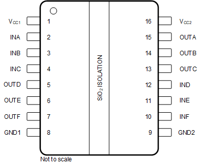
 Figure 4-1 DW Package, 16-Pin ワイド SOIC (Top View)
Table 4-1 Pin Functions
| PIN | TYPE(1) | DESCRIPTION | |
|---|---|---|---|
| NAME | NO. | ||
| VCC1 | 1 | P | Power supply, side 1 |
| INA | 2 | I | High-speed digital input, channel A |
| INB | 3 | I | High-speed digital input, channel B |
| INC | 4 | I | Low-speed control channel with automatic enable, channel C |
| OUTD | 5 | O | Digital output, channel D |
| OUTE | 6 | O | Digital output, channel E |
| OUTF | 7 | O | Digital output, channel F |
| GND1 | 8 | GND | Ground connection for VCC2, INA, INB, INC, OUTD, OUTE, and OUTF |
| GND2 | 9 | GND | Ground connection for VCC2, OUTA, OUTB, OUTC, IND, INE, and INF |
| INF | 10 | I | High-speed digital input, channel F |
| INE | 11 | I | High-speed digital input, channel E |
| IND | 12 | I | Low-speed control channel with automatic enable, channel D |
| OUTC | 13 | O | Digital output, channel C |
| OUTB | 14 | O | Digital output, channel B |
| OUTA | 15 | O | Digital output, channel A |
| VCC2 | 16 | P | Power supply, side 2 |
(1) I = input, O = output, P = power,
GND = ground