SLLS629M January 2006 – October 2024 ISO721 , ISO721M , ISO722 , ISO722M
PRODUCTION DATA
- 1
- 1 Features
- 2 Applications
- 3 Description
- 4 Device Comparison Table
- 5 Pin Configuration and Functions
-
6 Specifications
- 6.1 Absolute Maximum Ratings
- 6.2 ESD Ratings
- 6.3 Recommended Operating Conditions
- 6.4 Thermal Information
- 6.5 Power Ratings
- 6.6 Safety Limiting Values
- 6.7 Insulation Specifications
- 6.8 Safety-Related Certifications
- 6.9 Electrical Characteristics, 5 V, 3.3 V
- 6.10 Electrical Characteristics, 5 V
- 6.11 Switching Characteristics, 3.3 V, 5 V
- 6.12 Electrical Characteristics, 3.3 V, 5 V
- 6.13 Electrical Characteristics, 3.3 V
- 6.14 Switching Characteristics, 3.3 V
- 6.15 Switching Characteristics, 5 V, 3.3 V
- 6.16 Switching Characteristics, 5 V
- 6.17 Typical Characteristics
- 7 Parameter Measurement Information
- 8 Detailed Description
- 9 Application and Implementation
- 10Device and Documentation Support
- 11Revision History
- 12Mechanical, Packaging, and Orderable Information
7 Parameter Measurement Information
 Figure 7-1 Switching
Characteristic Test Circuit and Voltage Waveforms
 Figure 7-2 ISO722
Sleep-Mode High-Level Output Test Circuit and Voltage Waveforms
 Figure 7-3 ISO722
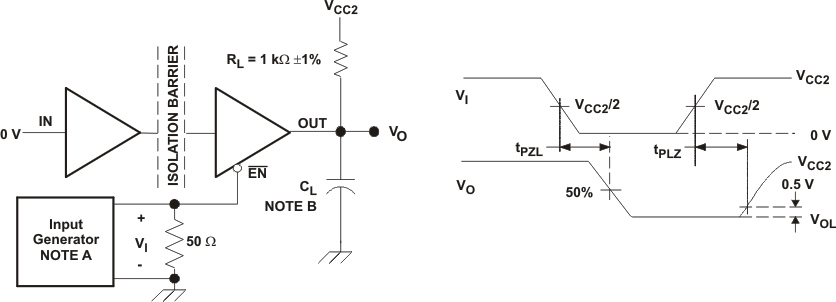
Sleep-Mode Low-Level Output Test Circuit and Voltage Waveforms
Figure 7-3 ISO722
Sleep-Mode Low-Level Output Test Circuit and Voltage WaveformsNote:
A: The input pulse is supplied by a generator having the following characteristics:
PRR ≤ 50 kHz, 50% duty cycle, tr ≤ 3 ns, tf ≤ 3 ns, ZO = 50 Ω.
B: CL = 15 pF ± 20% and includes instrumentation and fixture capacitance.

NOTE:
VI transition time is 100 ns.
Figure 7-4 Failsafe
Delay Time Test Circuit and Voltage Waveforms
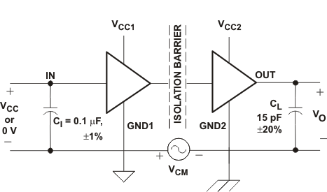
NOTE: Pass/fail
criterion is no change in VO.
Figure 7-5 Common-Mode Transient-Immunity Test Circuit and Voltage Waveform
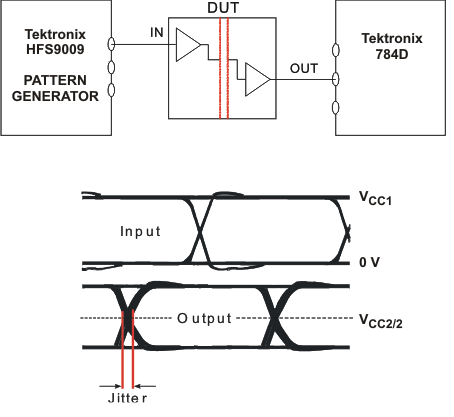
NOTE: Bit pattern
run length is 216 – 1. Transition time is 800 ps. NRZ data input has
no more than five consecutive 1s or 0s.
Figure 7-6 Peak-to-Peak Eye-Pattern Jitter Test Circuit and Voltage Waveform