SLLS629M January 2006 – October 2024 ISO721 , ISO721M , ISO722 , ISO722M
PRODUCTION DATA
- 1
- 1 Features
- 2 Applications
- 3 Description
- 4 Device Comparison Table
- 5 Pin Configuration and Functions
-
6 Specifications
- 6.1 Absolute Maximum Ratings
- 6.2 ESD Ratings
- 6.3 Recommended Operating Conditions
- 6.4 Thermal Information
- 6.5 Power Ratings
- 6.6 Safety Limiting Values
- 6.7 Insulation Specifications
- 6.8 Safety-Related Certifications
- 6.9 Electrical Characteristics, 5 V, 3.3 V
- 6.10 Electrical Characteristics, 5 V
- 6.11 Switching Characteristics, 3.3 V, 5 V
- 6.12 Electrical Characteristics, 3.3 V, 5 V
- 6.13 Electrical Characteristics, 3.3 V
- 6.14 Switching Characteristics, 3.3 V
- 6.15 Switching Characteristics, 5 V, 3.3 V
- 6.16 Switching Characteristics, 5 V
- 6.17 Typical Characteristics
- 7 Parameter Measurement Information
- 8 Detailed Description
- 9 Application and Implementation
- 10Device and Documentation Support
- 11Revision History
- 12Mechanical, Packaging, and Orderable Information
3 Description
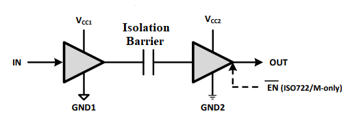
The ISO721, ISO721M, ISO722, and ISO722M devices are digital isolators with a logic input and output buffer separated by a silicon dioxide (SiO2) insulation barrier. This barrier provides galvanic isolation of up to 4000 VPK per VDE 0884-17. Used in conjunction with isolated power supplies, these devices prevent noise currents on a data bus or other circuits from entering the local ground, and interfering with or damaging sensitive circuitry.
A binary input signal is conditioned, translated to a balanced signal, then differentiated by the capacitive isolation barrier. Across the isolation barrier, a differential comparator receives the logic transition information, then sets or resets a flip-flop and the output circuit accordingly. A periodic update pulse is sent across the barrier to provide the proper dc level of the output.
If this dc-refresh pulse is not received for more than 4μs, the input is assumed to be unpowered or not being actively driven, and the failsafe circuit drives the output to a logic-high state.
These devices require two supply voltages of 3.3V, 5V, or any combination. All inputs are 5V tolerant when supplied from a 3.3V supply and all outputs are 4mA CMOS.
The ISO722 and ISO722M devices include an active-low output enable that when driven to a high logic level, places the output in a high-impedance state and turns off internal bias circuitry to conserve power.
The ISO721 and ISO722 devices have TTL input thresholds and a noise filter at the input that prevent transient pulses of up to 2 ns in duration from being passed to the output of the device.
The ISO721M and ISO722M devices have CMOS VCC / 2 input thresholds, but do not have the noise-filter and the additional propagation delay. These features of the ISO721M device also provide for reduced-jitter operation.
The ISO721, ISO721M, ISO722, and ISO722M devices are characterized for operation over the ambient temperature range of –40°C to +125°C.
| PART NUMBER(1) | PACKAGE | BODY SIZE (NOM) | PACKAGE SIZE(2) |
|---|---|---|---|
| ISO721 | D (SOIC, 8) | 4.90mm × 3.91mm | 4.9mm × 6mm |
| ISO721M | |||
| ISO722 | |||
| ISO722M |
 Simplified Schematic