JAJS331R July 2006 – October 2024 ISO7220A , ISO7220B , ISO7220C , ISO7220M , ISO7221A , ISO7221B , ISO7221C , ISO7221M
PRODUCTION DATA
- 1
- 1 特長
- 2 アプリケーション
- 3 概要
- 4 Pin Configuration and Functions
-
5 Specifications
- 5.1 Absolute Maximum Ratings
- 5.2 ESD Ratings
- 5.3 Recommended Operating Conditions
- 5.4 Thermal Information
- 5.5 Power Ratings
- 5.6 Insulation Specifications
- 5.7 Safety-Related Certifications
- 5.8 Safety Limiting Values
- 5.9 Electrical Characteristics—5-V VCC1 and VCC2 Supplies
- 5.10 Electrical Characteristics—5-V VCC1 and 3.3-V VCC2 Supply
- 5.11 Electrical Characteristics—3.3-V VCC1 and 5-V VCC2 Supply
- 5.12 Electrical Characteristics—3.3-V VCC1 and VCC2 Supplies
- 5.13 Electrical Characteristics—2.8-V VCC1 and VCC2 Supplies
- 5.14 Switching Characteristics—5-V VCC1 and VCC2 Supplies
- 5.15 Switching Characteristics—5-V VCC1 and 3.3-V VCC2 Supply
- 5.16 Switching Characteristics—3.3-VCC1 and 5-V VCC2 Supplies
- 5.17 Switching Characteristics—3.3-V VCC1 and VCC2 Supplies
- 5.18 Switching Characteristics—2.8-V VCC1 and VCC2 Supplies
- 5.19 Insulation Characteristics Curves
- 5.20 Typical Characteristics
- 6 Parameter Measurement Information
- 7 Detailed Description
- 8 Application and Implementation
- 9 Device and Documentation Support
- 10Revision History
- 11Mechanical, Packaging, and Orderable Information
8.2.2 Detailed Design Procedure
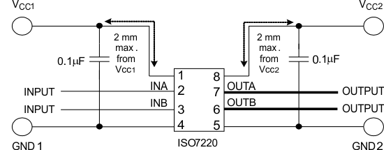
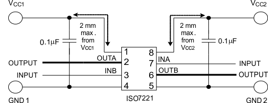
Figure 8-2 and Figure 8-3 show the hookup of a typical ISO7220x and ISO7221x circuit. The only external components are two bypass capacitors.
 Figure 8-2 Typical ISO7220x Circuit Hook-Up
 Figure 8-3 Typical ISO7221x Circuit Hook-Up