SLLSEU0G November 2016 – October 2024 ISO7740-Q1 , ISO7741-Q1 , ISO7742-Q1
PRODUCTION DATA
- 1
- 1 Features
- 2 Applications
- 3 Description
- 4 Pin Configuration and Functions
-
5 Specifications
- 5.1 Absolute Maximum Ratings
- 5.2 ESD Ratings
- 5.3 Recommended Operating Conditions
- 5.4 Thermal Information
- 5.5 Power Ratings
- 5.6 Insulation Specifications
- 5.7 Safety-Related Certifications
- 5.8 Safety Limiting Values
- 5.9 Electrical Characteristics—5-V Supply
- 5.10 Supply Current Characteristics—5-V Supply
- 5.11 Electrical Characteristics—3.3-V Supply
- 5.12 Supply Current Characteristics—3.3-V Supply
- 5.13 Electrical Characteristics—2.5-V Supply
- 5.14 Supply Current Characteristics—2.5-V Supply
- 5.15 Switching Characteristics—5-V Supply
- 5.16 Switching Characteristics—3.3-V Supply
- 5.17 Switching Characteristics—2.5-V Supply
- 5.18 Insulation Characteristics Curves
- 5.19 Typical Characteristics
- 6 Parameter Measurement Information
- 7 Detailed Description
- 8 Application and Implementation
- 9 Device and Documentation Support
- 10Revision History
- 11Mechanical, Packaging, and Orderable Information
パッケージ・オプション
デバイスごとのパッケージ図は、PDF版データシートをご参照ください。
メカニカル・データ(パッケージ|ピン)
- DBQ|16
- DW|16
サーマルパッド・メカニカル・データ
- DW|16
発注情報
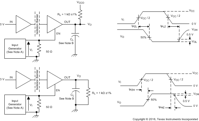
6 Parameter Measurement Information

A. The input pulse is supplied by a
generator having the following characteristics: PRR ≤ 50kHz, 50% duty cycle,
tr ≤ 3ns, tf ≤ 3ns, ZO = 50Ω. At the input,
50Ω resistor is required to terminate Input Generator signal. The 50Ω resistor
is not needed in actual application.
B. CL = 15pF and includes
instrumentation and fixture capacitance within ±20%.
Figure 6-1 Switching
Characteristics Test Circuit and Voltage Waveforms
A. The input pulse is supplied by a
generator having the following characteristics: PRR ≤ 10kHz, 50% duty cycle,
tr ≤ 3ns, tf ≤ 3ns, ZO = 50Ω.
tr ≤ 3ns, tf ≤ 3ns, ZO = 50Ω.
B. CL = 15pF and includes
instrumentation and fixture capacitance within ±20%.
Figure 6-2 Enable/Disable Propagation Delay Time Test Circuit and Waveform
A. CL = 15pF and includes
instrumentation and fixture capacitance within ±20%.
B. Power Supply Ramp Rate =
10mV/ns
Figure 6-3 Default
Output Delay Time Test Circuit and Voltage Waveforms
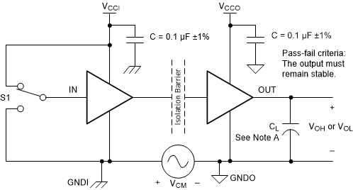
A. CL = 15pF and includes
instrumentation and fixture capacitance within ±20%.
Figure 6-4 Common-Mode Transient Immunity Test Circuit