JAJSLE7 May 2021 ISOS141-SEP
PRODUCTION DATA
- 1 特長
- 2 アプリケーション
- 3 概要
- 4 Revision History
- 5 Pin Configuration and Functions
-
6 Specifications
- 6.1 Absolute Maximum Ratings
- 6.2 ESD Ratings
- 6.3 Recommended Operating Conditions
- 6.4 Thermal Information
- 6.5 Power Ratings
- 6.6 Insulation Specifications
- 6.7 Safety-Related Certifications
- 6.8 Safety Limiting Values
- 6.9 Electrical Characteristics—5-V Supply
- 6.10 Supply Current Characteristics—5-V Supply
- 6.11 Electrical Characteristics—3.3-V Supply
- 6.12 Supply Current Characteristics—3.3-V Supply
- 6.13 Electrical Characteristics—2.5-V Supply
- 6.14 Supply Current Characteristics—2.5-V Supply
- 6.15 Switching Characteristics—5-V Supply
- 6.16 Switching Characteristics—3.3-V Supply
- 6.17 Switching Characteristics—2.5-V Supply
- 6.18 Insulation Characteristics Curves
- 6.19 Typical Characteristics
- 7 Operating Life Deration
- 8 Parameter Measurement Information
- 9 Detailed Description
- 10Application and Implementation
- 11Power Supply Recommendations
- 12Layout
- 13Device and Documentation Support
- 14Mechanical, Packaging, and Orderable Information
7 Operating Life Deration
The information in this section is provided solely for your convenience and does not extend or modify the warranty provided under TI's standard terms and conditions for TI semiconductor products.

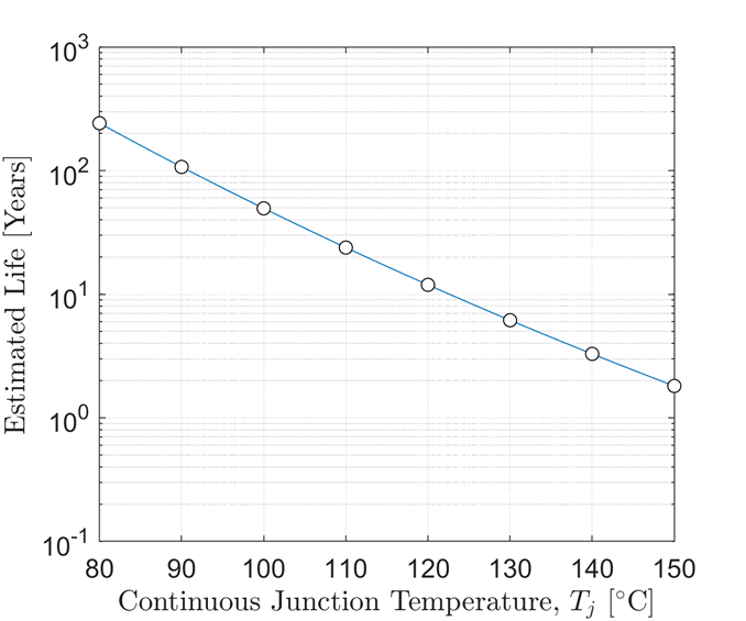
- Silicon operating life design goal is 100000 power-on hours (POH) at 105 °C junction temperature (does not include package interconnect life).
- The predicted operating lifetime versus junction temperature is based on reliability modeling using wirebond lifetime as the dominant failure mechanism affecting device wear out for the specific device process and design characteristics.