JAJSLI4A May 2021 – December 2021 ISOW1044
PRODUCTION DATA
- 1 特長
- 2 アプリケーション
- 3 概要
- 4 Revision History
- 5 概要 (続き)
- 6 Device Comparison Table
- 7 Pin Configuration and Functions
-
8 Specifications
- 8.1 Absolute Maximum Ratings
- 8.2 ESD Ratings
- 8.3 Recommended Operating Conditions
- 8.4 ThermalInformation
- 8.5 Power Ratings
- 8.6 Insulation Specifications
- 8.7 Safety-Related Certifications
- 8.8 Safety Limiting Values
- 8.9 Electrical Characteristics
- 8.10 Supply Current Characteristics
- 8.11 Switching Characteristics
- 8.12 Insulation Characteristics Curves
- 8.13 Typical Characteristics
- 9 Parameter Measurement Information
- 10Detailed Description
- 11Application and Implementation
- 12Power Supply Recommendations
- 13Layout
- 14Device and Documentation Support
- 15Mechanical, Packaging, and Orderable Information
10.6.1 CAN Bus States
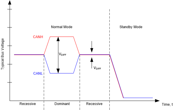
The CAN bus has two logical states during operation: recessive and dominant. A dominant bus state occurs when the bus is driven differentially and corresponds to a logic low on the TXD and RXD pins. A recessive bus state occurs when the bus is biased to VCC/2 via the high-resistance internal input resistors (RIN) of the receiver and corresponds to a logic high on the TXD and RXD pins.
A dominant state overwrites the recessive state during arbitration. Multiple CAN nodes may be transmitting a dominant bit at the same time during arbitration, and in this case the differential voltage of the bus is greater than the differential voltage of a single driver.
The ISOW1044 transceiver implements a standby (STB ) mode which enables a third bus state where the bus pins are weakly biased to ground via the high resistance internal resistors of the receiver.
 Figure 10-4 Bus
States (Physical Bit Representation)
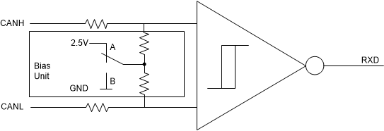
 Figure 10-5 Simplified Recessive Common Mode Bias and Receiver