JAJSLI4A May 2021 – December 2021 ISOW1044
PRODUCTION DATA
- 1 特長
- 2 アプリケーション
- 3 概要
- 4 Revision History
- 5 概要 (続き)
- 6 Device Comparison Table
- 7 Pin Configuration and Functions
-
8 Specifications
- 8.1 Absolute Maximum Ratings
- 8.2 ESD Ratings
- 8.3 Recommended Operating Conditions
- 8.4 ThermalInformation
- 8.5 Power Ratings
- 8.6 Insulation Specifications
- 8.7 Safety-Related Certifications
- 8.8 Safety Limiting Values
- 8.9 Electrical Characteristics
- 8.10 Supply Current Characteristics
- 8.11 Switching Characteristics
- 8.12 Insulation Characteristics Curves
- 8.13 Typical Characteristics
- 9 Parameter Measurement Information
- 10Detailed Description
- 11Application and Implementation
- 12Power Supply Recommendations
- 13Layout
- 14Device and Documentation Support
- 15Mechanical, Packaging, and Orderable Information
10.6.3 TXD Dominant Timeout (DTO)
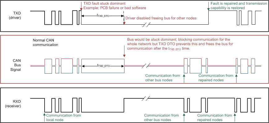
The TXD DTO circuit prevents the transceiver from blocking network communication in the event of a hardware or software failure where the TXD pin is held dominant longer than the timeout period, tTXD_DTO. The DTO circuit timer starts on a falling edge on the TXD pin. The DTO circuit disables the CAN bus driver if no rising edge occurs before the timeout period expires, which frees the bus for communication between other nodes on the network. The CAN driver is activated again when a recessive signal occurs on the TXD pin, clearing the TXD DTO condition. The receiver and RXD pin still reflect activity on the CAN bus, and the bus terminals are biased to the recessive level during a TXD dominant timeout.
 Figure 10-6 Example Timing Diagram for TXD DTO
The minimum dominant TXD time (tTXD_DTO) allowed by the TXD DTO circuit limits the minimum possible transmitted data rate of the device. The CAN protocol allows a maximum of eleven successive dominant bits (on TXD) for the worst case, where five successive dominant bits are followed immediately by an error frame. This, along with the tTXD_DTO minimum, limits the minimum data rate. Calculate the minimum transmitted data rate with Equation 1.