JAJSJ74B August 2021 – August 2023 JFE2140
PRODUCTION DATA
- 1
- 1 特長
- 2 アプリケーション
- 3 概要
- 4 Revision History
- 5 Pin Configuration and Functions
- 6 Specifications
- 7 Parameter Measurement Information
- 8 Detailed Description
- 9 Application and Implementation
- 10Device and Documentation Support
- 11Mechanical, Packaging, and Orderable Information
パッケージ・オプション
メカニカル・データ(パッケージ|ピン)
サーマルパッド・メカニカル・データ
- DSG|8
発注情報
9.1.3 Common-Source Amplifier
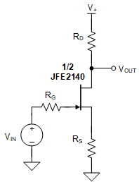
The common-source amplifier is a commonly used open-loop gain stage for JFET amplifiers, the basic circuit is shown in Figure 9-3.
 Figure 9-3 Common-Source
Amplifier
Figure 9-3 Common-Source
AmplifierThe equation for gain of the circuit in Figure 9-3 is shown in Equation 1.
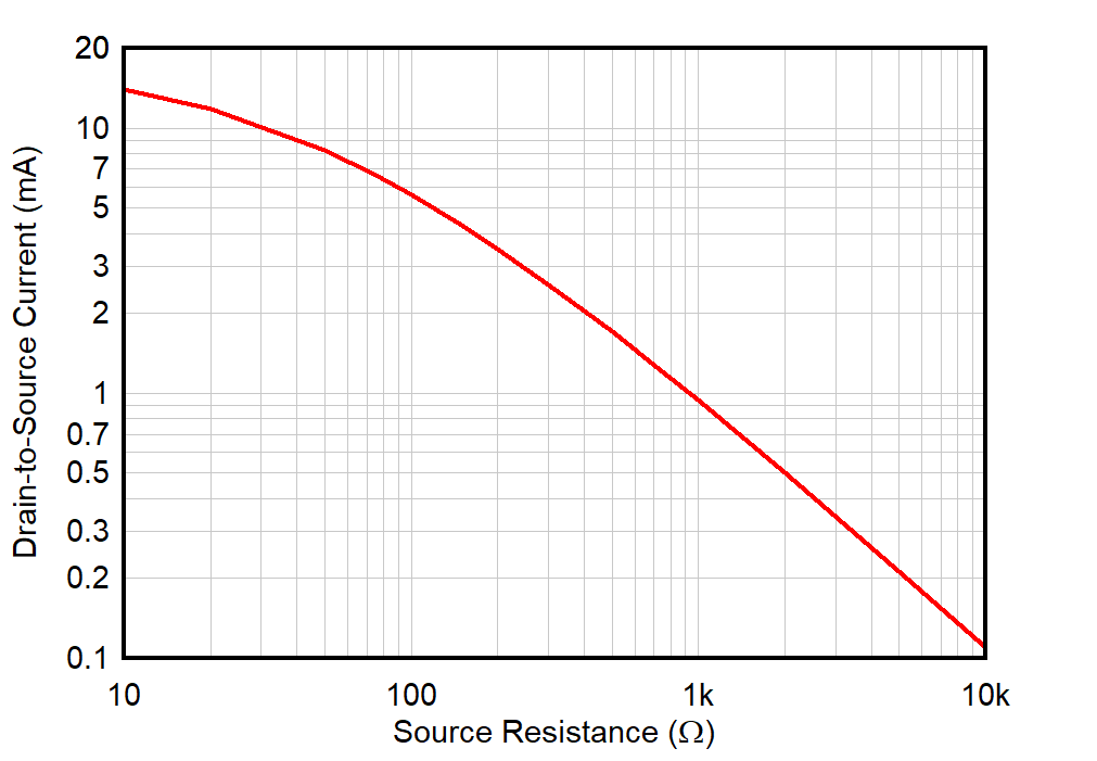
Generally, higher gain results in improved noise performance. Gain increases as the bias current is increased as a result of increasing gm (see Figure 6-4). As a result, the input-referred noise decreases as bias current is increased (see Figure 6-14). Any JFET design must make a tradeoff between current consumption and noise performance. The JFE2140, however, delivers significantly lower noise performance than most operational amplifiers at the same current consumption. The bias current (IDS) is set by the value of the source resistor, RS, and the threshold voltage, VT, of the JFE2140. For JFETs, this threshold voltage is equivalent to the gate-to-source cutoff voltage, VGSC. A graph showing nominal IDS vs RS is shown in Figure 9-4.
 Figure 9-4 Drain-to-Source Current vs
RS, VDS = 5 V
Figure 9-4 Drain-to-Source Current vs
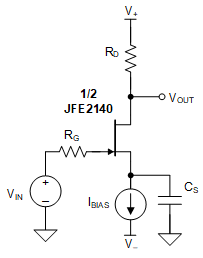
RS, VDS = 5 VThe bias current varies according to the resistor and threshold voltage tolerances. Additionally, thermal noise associated with RS couples directly into the gain of the circuit, degrading the overall noise performance. To improve the circuit in Figure 9-5, use a current-source biasing scheme. Current-source biasing removes the JFET threshold variation from the biasing scheme, and allows for lower-value filtering capacitance (CS) for equivalent filtering due to the high output impedance of current sources.
 Figure 9-5 Common-Source Amplifier With
Current-Source Biasing