JAJSJ74B August   2021  – August 2023 JFE2140

PRODUCTION DATA  

  1.   1
  2. 特長
  3. アプリケーション
  4. 概要
  5. Revision History
  6. Pin Configuration and Functions
  7. Specifications
    1. 6.1 Absolute Maximum Ratings
    2. 6.2 ESD Ratings
    3. 6.3 Recommended Operating Conditions
    4. 6.4 Thermal Information
    5. 6.5 Electrical Characteristics
    6. 6.6 Typical Characteristics
  8. Parameter Measurement Information
    1. 7.1 AC Measurement Configurations
  9. Detailed Description
    1. 8.1 Overview
    2. 8.2 Functional Block Diagram
    3. 8.3 Feature Description
      1. 8.3.1 Precision Matching
      2. 8.3.2 Ultra-Low Noise
      3. 8.3.3 Low Gate Current
      4. 8.3.4 Input Protection
    4. 8.4 Device Functional Modes
  10. Application and Implementation
    1. 9.1 Application Information
      1. 9.1.1 Input Protection Diodes
      2. 9.1.2 Cascode Configuration
      3. 9.1.3 Common-Source Amplifier
      4. 9.1.4 Composite Amplifiers
    2. 9.2 Typical Applications
      1. 9.2.1 Low-Noise, Low-Power, High-Input-Impedance Composite Amplifier
        1. 9.2.1.1 Design Requirements
        2. 9.2.1.2 Detailed Design Procedure
        3. 9.2.1.3 Application Curves
      2. 9.2.2 Differential Front-End Design
        1. 9.2.2.1 Application Curves
    3. 9.3 Power Supply Recommendations
    4. 9.4 Layout
      1. 9.4.1 Layout Guidelines
      2. 9.4.2 Layout Example
  11. 10Device and Documentation Support
    1. 10.1 Device Support
      1. 10.1.1 Development Support
        1. 10.1.1.1 PSpice® for TI
        2. 10.1.1.2 TINA-TI™シミュレーション・ソフトウェア (無償ダウンロード)
        3. 10.1.1.3 TI のリファレンス・デザイン
        4. 10.1.1.4 フィルタ設計ツール
    2. 10.2 Documentation Support
      1. 10.2.1 Related Documentation
    3. 10.3 ドキュメントの更新通知を受け取る方法
    4. 10.4 サポート・リソース
    5. 10.5 Trademarks
    6. 10.6 静電気放電に関する注意事項
    7. 10.7 用語集
  12. 11Mechanical, Packaging, and Orderable Information

パッケージ・オプション

メカニカル・データ(パッケージ|ピン)
サーマルパッド・メカニカル・データ
発注情報

Cascode Configuration

The JFE2140 can be configured as a cascoded JFET front end. Cascode refers to using a second transistor in-series with the input transistor; see Figure 9-2 for an example.
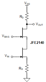
GUID-20210810-SS0I-QP9D-PM6L-G07J4NQDQ7TJ-low.gif Figure 9-2 JFE2140 connected in Cascode Configuration

Using a cascode configuration, as shown in Figure 9-2, increases the output impedance of the stage, resulting in higher gain, as well as buffers the input node from gate current that flows when the VDS voltages are higher. The VBIAS node must be forced to a voltage greater than what is required to allow both JFETs to remain in the saturated region. A JFET is not required to be used as the cascode device; the benefits of cascoding can be realized with other transistor types, while still maintaining the low-noise, high-impedance benefits of the JFE2140.