JAJSJ74B August   2021  – August 2023 JFE2140

PRODUCTION DATA  

  1.   1
  2. 特長
  3. アプリケーション
  4. 概要
  5. Revision History
  6. Pin Configuration and Functions
  7. Specifications
    1. 6.1 Absolute Maximum Ratings
    2. 6.2 ESD Ratings
    3. 6.3 Recommended Operating Conditions
    4. 6.4 Thermal Information
    5. 6.5 Electrical Characteristics
    6. 6.6 Typical Characteristics
  8. Parameter Measurement Information
    1. 7.1 AC Measurement Configurations
  9. Detailed Description
    1. 8.1 Overview
    2. 8.2 Functional Block Diagram
    3. 8.3 Feature Description
      1. 8.3.1 Precision Matching
      2. 8.3.2 Ultra-Low Noise
      3. 8.3.3 Low Gate Current
      4. 8.3.4 Input Protection
    4. 8.4 Device Functional Modes
  10. Application and Implementation
    1. 9.1 Application Information
      1. 9.1.1 Input Protection Diodes
      2. 9.1.2 Cascode Configuration
      3. 9.1.3 Common-Source Amplifier
      4. 9.1.4 Composite Amplifiers
    2. 9.2 Typical Applications
      1. 9.2.1 Low-Noise, Low-Power, High-Input-Impedance Composite Amplifier
        1. 9.2.1.1 Design Requirements
        2. 9.2.1.2 Detailed Design Procedure
        3. 9.2.1.3 Application Curves
      2. 9.2.2 Differential Front-End Design
        1. 9.2.2.1 Application Curves
    3. 9.3 Power Supply Recommendations
    4. 9.4 Layout
      1. 9.4.1 Layout Guidelines
      2. 9.4.2 Layout Example
  11. 10Device and Documentation Support
    1. 10.1 Device Support
      1. 10.1.1 Development Support
        1. 10.1.1.1 PSpice® for TI
        2. 10.1.1.2 TINA-TI™シミュレーション・ソフトウェア (無償ダウンロード)
        3. 10.1.1.3 TI のリファレンス・デザイン
        4. 10.1.1.4 フィルタ設計ツール
    2. 10.2 Documentation Support
      1. 10.2.1 Related Documentation
    3. 10.3 ドキュメントの更新通知を受け取る方法
    4. 10.4 サポート・リソース
    5. 10.5 Trademarks
    6. 10.6 静電気放電に関する注意事項
    7. 10.7 用語集
  12. 11Mechanical, Packaging, and Orderable Information

パッケージ・オプション

メカニカル・データ(パッケージ|ピン)
サーマルパッド・メカニカル・データ
発注情報

Device Functional Modes

The JFE2140 functionality is identical to standard N-channel depletion JFET devices. The gate-to-source (VGS) voltage, drain-to-source voltage (VDS) and drain-to-source current (IDS) determine the region of operation.

  • For VGS < VGSC: JFE2140 conduction channel is closed; IDS is only determined by junction leakage current.
  • For VGS > VGSC: Two modes of operation can exist depending on VDS. When VDS is less than the linear (saturation) region threshold (see Figure 9-2), the device operates in the linear region, meaning that the device behaves as a resistor connected from drain-to-source with minimal variation from any changes in VGS. When VDS is greater than the linear (saturation) region threshold, IDS has a strong dependance on VGS, where the relationship is described by the parameter gm.
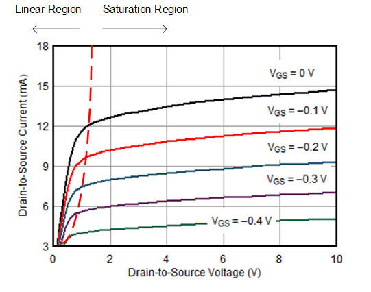
GUID-20210810-SS0I-XN9N-PVWD-TBDTRXSP68RT-low.gif Figure 8-1 VDS vs IDS