JAJSI63 November 2019 LDC1001-Q1
PRODUCTION DATA.
- 1 特長
- 2 アプリケーション
- 3 概要
- 4 改訂履歴
- 5 Pin Configuration and Functions
- 6 Specifications
-
7 Detailed Description
- 7.1 Overview
- 7.2 Functional Block Diagram
- 7.3 Feature Description
- 7.4 Device Functional Modes
- 7.5 Programming
- 7.6
Register Map
- 7.6.1
Register Description
- 7.6.1.1 Revision ID (offset = 0x00) [reset = 0x80]
- 7.6.1.2 Rp_MAX (offset = 0x01) [reset = 0x0E]
- 7.6.1.3 Rp_MIN (offset = 0x02) [reset = 0x14]
- 7.6.1.4 Sensor Frequency (offset = 0x03) [reset = 0x45]
- 7.6.1.5 LDC Configuration (offset = 0x04) [reset = 0x1B]
- 7.6.1.6 Clock Configuration (offset = 0x05) [reset = 0x01]
- 7.6.1.7 Comparator Threshold High LSB (offset = 0x06) [reset = 0xFF]
- 7.6.1.8 Comparator Threshold High MSB (offset = 0x07) [reset = 0xFF]
- 7.6.1.9 Comparator Threshold Low LSB (offset = 0x08) [reset = 0x00]
- 7.6.1.10 Comparator Threshold Low MSB (offset = 0x09) [reset = 0x00]
- 7.6.1.11 INTB Pin Configuration (offset = 0x0A) [reset = 0x00]
- 7.6.1.12 Power Configuration (offset = 0x0B) [reset = 0x00]
- 7.6.1.13 Status (offset = 0x20) [reset = NA]
- 7.6.1.14 Proximity Data LSB (offset = 0x21) [reset = NA]
- 7.6.1.15 Proximity Data MSB (offset = 0x22) [reset = NA]
- 7.6.1.16 Frequency Counter LSB (offset = 0x23) [reset = NA]
- 7.6.1.17 Frequency Counter Mid-Byte (offset = 0x24) [reset = NA]
- 7.6.1.18 Frequency Counter MSB (offset = 0x25) [reset = NA]
- 7.6.1
Register Description
- 8 Application and Implementation
- 9 Power Supply Recommendations
- 10Layout
- 11デバイスおよびドキュメントのサポート
- 12メカニカル、パッケージ、および注文情報
7.3.1 Inductive Sensing
An alternating current (AC) flowing through a coil generates an AC magnetic field. If a conductive material, such as a metal target, is brought into the vicinity of the coil, this magnetic field induces circulating currents (eddy currents) on the surface of the target. These eddy currents are a function of the distance, size, and composition of the target. These eddy currents then generate a magnetic field that opposes the original field generated by the coil. This mechanism is best compared to a transformer, where the coil is the primary core and the eddy current is the secondary core. The inductive coupling between both cores depends on distance and shape. Hence the resistance and inductance of the secondary core (eddy current), shows up as a distant dependent resistive and inductive component on the primary side (coil). Figure 5 through Figure 8 show a simplified circuit model.
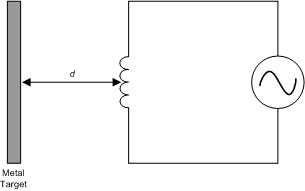 Figure 5. Inductor With a Metal Target
 Eddy currents generated on the surface of the target can be modeled as a transformer as shown in Figure 6. The coupling between the primary and secondary coils is a function of the distance and characteristics of the conductor. In Figure 6, the inductance Ls is the inductance of the coil, and rs is the parasitic series resistance of the coil. The inductance L(d), which is a function of distance, d, is the coupled inductance of the metal target. Likewise, R(d) is the parasitic resistance of the eddy currents.
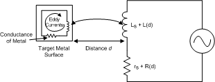 Figure 6. Metal Target Modeled as L and R With Circulating Eddy Currents
 Generating an alternating magnetic field with just an inductor consumes a large amount of power. This power consumption can be reduced by adding a parallel capacitor, turning the right part of Figure 6 into a resonator as shown in Figure 7. In this manner the power consumption is reduced to the eddy and inductor losses rs + R(d) only.
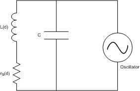 Figure 7. LC Tank Connected to Oscillator
 The LDC1001-Q1 device does not directly measure the series resistance. Instead, the device measures the equivalent parallel resonance impedance RP (see Figure 8). This representation is equivalent to the representation shown in Figure 8, where the parallel resonance impedance RP(d) is given by Equation 1.
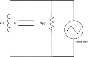 Figure 8. Equivalent Resistance of rs in Parallel With LC Tank
 Figure 9 shows the variation in RP as a function of distance for a 14-mm diameter PCB coil (23 turns, 4-mil trace width, 4-mil spacing between trace, 1-oz copper thickness, FR4). The target metal used is a stainless steel 2-mm thick.
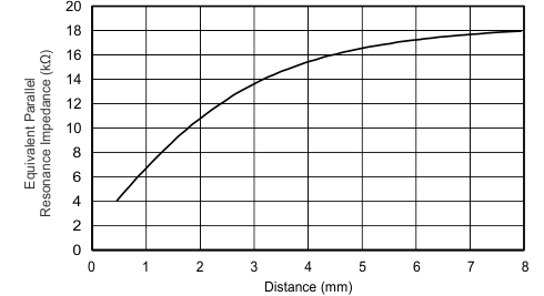 Figure 9. Typical RP vs Distance With a 14-mm PCB Coil