JAJSF29A December 2014 – March 2018 LDC1312 , LDC1314
PRODUCTION DATA.
- 1 特長
- 2 アプリケーション
- 3 概要
- 4 改訂履歴
- 5 Pin Configuration and Functions
- 6 Specifications
-
7 Detailed Description
- 7.1 Overview
- 7.2 Functional Block Diagram
- 7.3 Feature Description
- 7.4 Device Functional Modes
- 7.5 Programming
- 7.6
Register Maps
- 7.6.1 Register List
- 7.6.2 Address 0x00, DATA0
- 7.6.3 Address 0x02, DATA1
- 7.6.4 Address 0x04, DATA2 (LDC1314 only)
- 7.6.5 Address 0x06, DATA3 (LDC1314 only)
- 7.6.6 Address 0x08, RCOUNT0
- 7.6.7 Address 0x09, RCOUNT1
- 7.6.8 Address 0x0A, RCOUNT2 (LDC1314 only)
- 7.6.9 Address 0x0B, RCOUNT3 (LDC1314 only)
- 7.6.10 Address 0x0C, OFFSET0
- 7.6.11 Address 0x0D, OFFSET1
- 7.6.12 Address 0x0E, OFFSET2 (LDC1314 only)
- 7.6.13 Address 0x0F, OFFSET3 (LDC1314 only)
- 7.6.14 Address 0x10, SETTLECOUNT0
- 7.6.15 Address 0x11, SETTLECOUNT1
- 7.6.16 Address 0x12, SETTLECOUNT2 (LDC1314 only)
- 7.6.17 Address 0x13, SETTLECOUNT3 (LDC1314 only)
- 7.6.18 Address 0x14, CLOCK_DIVIDERS0
- 7.6.19 Address 0x15, CLOCK_DIVIDERS1
- 7.6.20 Address 0x16, CLOCK_DIVIDERS2 (LDC1314 only)
- 7.6.21 Address 0x17, CLOCK_DIVIDERS3 (LDC1314 only)
- 7.6.22 Address 0x18, STATUS
- 7.6.23 Address 0x19, ERROR_CONFIG
- 7.6.24 Address 0x1A, CONFIG
- 7.6.25 Address 0x1B, MUX_CONFIG
- 7.6.26 Address 0x1C, RESET_DEV
- 7.6.27 Address 0x1E, DRIVE_CURRENT0
- 7.6.28 Address 0x1F, DRIVE_CURRENT1
- 7.6.29 Address 0x20, DRIVE_CURRENT2 (LDC1314 only)
- 7.6.30 Address 0x21, DRIVE_CURRENT3 (LDC1314 only)
- 7.6.31 Address 0x7E, MANUFACTURER_ID
- 7.6.32 Address 0x7F, DEVICE_ID
-
8 Application and Implementation
- 8.1
Application Information
- 8.1.1 Conductive Objects in a Time-Varying EM Field
- 8.1.2 L-C Resonators
- 8.1.3 Multi-Channel and Single Channel Operation
- 8.1.4 Sensor Conversion Time
- 8.1.5 Sensor Current Drive Configuration
- 8.1.6 Clocking Architecture
- 8.1.7 Input Deglitch Filter
- 8.1.8 Device Status Registers
- 8.1.9 Multi-Channel Data Readback
- 8.2 Typical Application
- 8.1
Application Information
- 9 Power Supply Recommendations
- 10Layout
- 11デバイスおよびドキュメントのサポート
- 12メカニカル、パッケージ、および注文情報
パッケージ・オプション
メカニカル・データ(パッケージ|ピン)
- RGH|16
サーマルパッド・メカニカル・データ
- RGH|16
発注情報
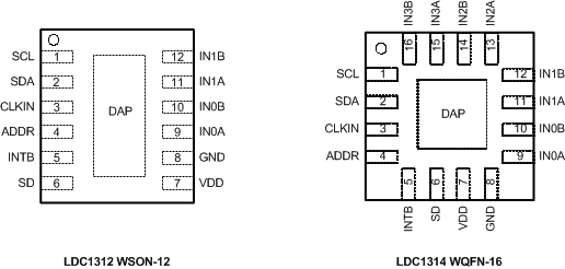
5 Pin Configuration and Functions
DNT and RGH Packages
Top View

Pin Functions
| PIN | TYPE(1) | DESCRIPTION | |
|---|---|---|---|
| NAME | NO. | ||
| SCL | 1 | I | I2C Clock input. Open drain output; requires resistive pullup to logic high level. |
| SDA | 2 | I/O | I2C Data input/output. Open drain output; requires resistive pullup to logic high level. |
| CLKIN | 3 | I | External Reference Clock input. Tie this pin to GND if internal oscillator is used. |
| ADDR | 4 | I | I2C Address selection pin: when ADDR=L, I2C address = 0x2A, when ADDR=H, I2C address = 0x2B. This input must not be allowed to float. |
| INTB | 5 | O | Configurable Interrupt output pin. Push-pull output; does not require pullup. |
| SD | 6 | I | Shutdown input: set SD = L for normal operation, set SD=H for inactive mode. This input must not be allowed to float. |
| VDD | 7 | P | Power Supply |
| GND | 8 | G | Ground |
| IN0A | 9 | A | External LC sensor 0 connection |
| IN0B | 10 | A | External LC sensor 0 connection |
| IN1A | 11 | A | External LC sensor 1 connection |
| IN1B | 12 | A | External LC sensor 1 connection |
| IN2A | 13 | A | External LC sensor 2 connection (LDC1314 only) |
| IN2B | 14 | A | External LC sensor 2 connection (LDC1314 only) |
| IN3A | 15 | A | External LC sensor 3 connection (LDC1314 only) |
| IN3B | 16 | A | External LC sensor 3 connection (LDC1314 only) |
| DAP(2) | DAP | N/A | Connect to Ground |
(1) I = Input, O = Output, P=Power, G=Ground, A=Analog
(2) There is an internal electrical connection between the exposed Die Attach Pad (DAP) and the GND pin of the device. Although the DAP can be left floating, for best performance the DAP should be connected to the same potential as the device's GND pin. Do not use the DAP as the primary ground for the device. The device GND pin must always be connected to ground.