JAJSDB3 June 2017 LF298-MIL
PRODUCTION DATA.
- 1 特長
- 2 アプリケーション
- 3 概要
- 4 改訂履歴
- 5 Pin Configuration and Functions
- 6 Specifications
- 7 Parameter Measurement Information
- 8 Detailed Description
-
9 Application and Implementation
- 9.1 Application Information
- 9.2
Typical Applications
- 9.2.1 X1000 Sample and Hold
- 9.2.2 Sample and Difference Circuit
- 9.2.3 Ramp Generator With Variable Reset Level
- 9.2.4 Integrator With Programmable Reset Level
- 9.2.5 Output Holds at Average of Sampled Input
- 9.2.6 Increased Slew Current
- 9.2.7 Reset Stabilized Amplifier
- 9.2.8 Fast Acquisition, Low Droop Sample and Hold
- 9.2.9 Synchronous Correlator for Recovering Signals Below Noise Level
- 9.2.10 2-Channel Switch
- 9.2.11 DC and AC Zeroing
- 9.2.12 Staircase Generator
- 9.2.13 Differential Hold
- 9.2.14 Capacitor Hysteresis Compensation
- 10Power Supply Recommendations
- 11Layout
- 12デバイスおよびドキュメントのサポート
- 13メカニカル、パッケージ、および注文情報
9 Application and Implementation
NOTE
Information in the following applications sections is not part of the TI component specification, and TI does not warrant its accuracy or completeness. TI’s customers are responsible for determining suitability of components for their purposes. Customers should validate and test their design implementation to confirm system functionality.
9.1 Application Information
9.1.1 Hold Capacitor
Hold step, acquisition time, and droop rate are the major trade-offs in the selection of a hold capacitor value. Size and cost may also become important for larger values. Use of the curves included with this data sheet should be helpful in selecting a reasonable value of capacitance.
A significant source of error in an accurate sample and hold circuit is dielectric absorption in the hold capacitor. A mylar cap, for instance, may sag back up to 0.2% after a quick change in voltage. A long sample time is required before the circuit can be put back into the hold mode with this type of capacitor. Dielectrics with very low hysteresis are polystyrene, polypropylene, and Teflon. Other types such as mica and polycarbonate are not nearly as good. The advantage of polypropylene over polystyrene is that it extends the maximum ambient temperature from 85°C to 100°C. Most ceramic capacitors are unusable with > 1% hysteresis. Ceramic NPO or COG capacitors are now available for 125°C operation and also have low dielectric absorption. For more exact data, see Figure 2. The hysteresis numbers on the curve are final values, taken after full relaxation. The hysteresis relaxation time constant in polypropylene, for instance, is 10 to 50 ms. If A-to-D conversion can be made within 1 ms, hysteresis error will be reduced by a factor of ten.
9.1.2 DC and AC Zeroing
DC zeroing is accomplished by connecting the offset adjust pin to the wiper of a 1-kΩ potentiometer, which has one end tied to V+ and the other end tied through a resistor to ground. The resistor should be selected to give approximately 0.6 mA through the 1-kΩ potentiometer.
AC zeroing (hold step zeroing) can be obtained by adding an inverter with the adjustment pot tied input to output. A 10-pF capacitor from the wiper to the hold capacitor will give ±4-mV hold step adjustment with a 0.01-µF hold capacitor and 5-V logic supply. For larger logic swings, a smaller capacitor (< 10 pF) may be used.
9.1.3 Logic Rise Time
Slower signals will cause excessive hold step. If a R/C network is used in front of the logic input for signal delay, calculate the slope of the waveform at the threshold point to ensure that it is at least 1.0 V/µs.
9.1.4 Sampling Dynamic Signals
Sample error to moving input signals probably causes more confusion among sample-and-hold users than any other parameter. The primary reason for this is that many users make the assumption that the sample and hold amplifier is truly locked on to the input signal while in the sample mode. In actuality, there are finite phase delays through the circuit creating an input-output differential for fast moving signals. In addition, although the output may have settled, the hold capacitor has an additional lag due to the 300-Ω series resistor on the chip. This means that at the moment the hold command arrives, the hold capacitor voltage may be somewhat different than the actual analog input. The effect of these delays is opposite to the effect created by delays in the logic which switches the circuit from sample to hold. For example, consider an analog input of 20 Vp–p at 10 kHz. Maximum dV/dt is 0.6 V/µs. With no analog phase delay and 100-ns logic delay, one could expect up to (0.1 µs) (0.6V/µs) = 60 mVerror if the hold signal arrived near maximum dV/dt of the input. A positive-going input would give a
60-mV error. Now assume a 1-MHz (3-dB) bandwidth for the overall analog loop. This generates a phase delay of 160 ns. If the hold capacitor sees this exact delay, then error due to analog delay will be (0.16 µs) (0.6 V/µs) = –96 mV. Total output error is 60 mV (digital) –96 mV (analog) for a total of –36 mV. To add to the confusion, analog delay is proportioned to hold capacitor value while digital delay remains constant. A family of curves (dynamic sampling error) is included to help estimate errors.
Figure 1 has been included for sampling conditions where the input is steady during the sampling period, but may experience a sudden change nearly coincident with the hold command. This curve is based on a 1-mV error fed into the output.
Figure 6 indicates the time required for the output to settle to 1 mV after the hold command.
9.1.5 Digital Feedthrough
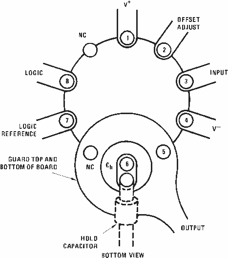
Fast rise time logic signals can cause hold errors by feeding externally into the analog input at the same time the amplifier is put into the hold mode. To minimize this problem, board layout should keep logic lines as far as possible from the analog input and the Ch pin. Grounded guarding traces may also be used around the input line, especially if it is driven from a high impedance source. Reducing high amplitude logic signals to 2.5 V will also help.
9.2 Typical Applications
9.2.1 X1000 Sample and Hold
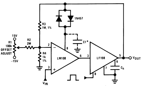
The circuit configuration in Figure 25 shows how to incorporate an amplification factor of 1000 into the sample and hold stage. This may be particularly useful if the input signal has a very low amplitude. Equation 1 provides the appropriate value of capacitance for the COMP 2 pin capacitance of the LM108.
| *For lower gains, the LM108 must be frequency compensated |

9.2.1.1 Design Requirements
Assume an unbuffered analog to digital converter with 1-Vpp dynamic range is used in a system which needs to sample an input signal with only 1-mVpp amplitude. Using the device and LM108, connect the input signal so that the maximum dynamic range is used by the 1-Vpp data converter.
9.2.1.2 Detailed Design Procedure
Connect the device and LM108 as shown in Figure 25. To maximize the dynamic range of 1 Vpp a gain factor of 1000x is needed. Set R3 to 1 MΩ and R4 to 1 kΩ to give a noninverting gain of 1001. The calculated value of C1 is 0.1 pF according to Equation 1, which is negligibly small and may be left off of the design.
9.2.1.3 Application Curves
The feedthrough rejection ratio of the LF298-MIL is extremely good and provides good isolation for a wide variety of hold capacitors as Figure 26 shows. Additionally, the output transient settles almost completely after 0.8 µs and would be ready to sample as shown in Figure 27.
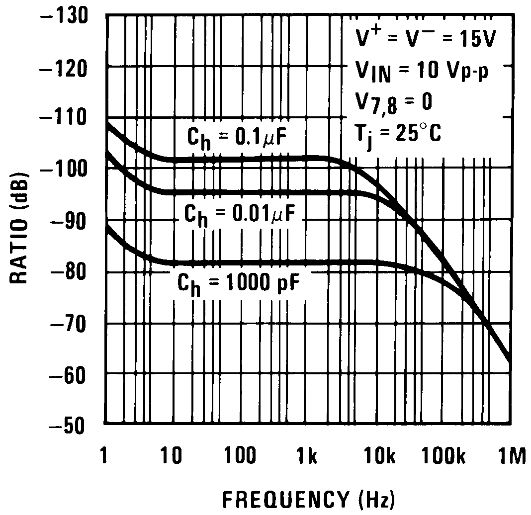 Figure 26. Feedthrough Rejection Ratio (Hold Mode)
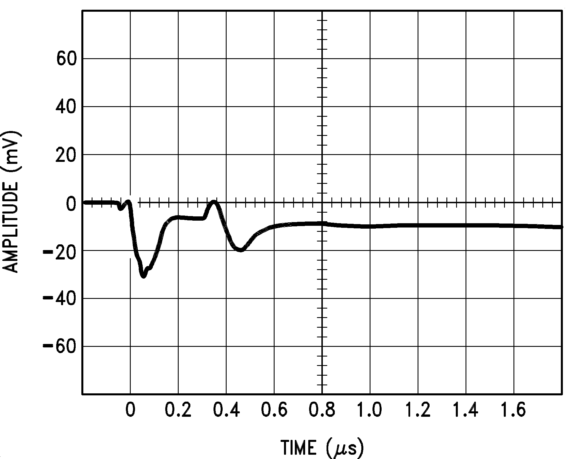 Figure 27. Output Transient at Start of Hold Mode
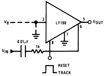
9.2.2 Sample and Difference Circuit
The device may be used as a sample and difference circuit as shown in Figure 28 where the output follows the input in hold mode.
9.2.3 Ramp Generator With Variable Reset Level
The circuit configuration shown in Figure 29 generates a ramp signal with variable reset level. The rise or fall time may be computed by Equation 2.
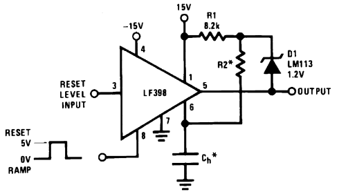 Figure 29. Ramp Generator With Variable Reset Level

9.2.4 Integrator With Programmable Reset Level
The device may be used with LM308 to create an integrator circuit with programmable reset level as shown in Figure 30. The integrated output voltage in hold mode is computed with Equation 3.
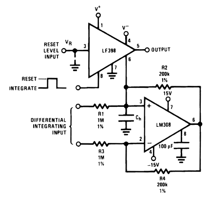 Figure 30. Integrator With Programmable Reset Level

9.2.5 Output Holds at Average of Sampled Input
The device can be used to identify the average value of the input signal and hold the corresponding voltage on the output. Connect Rh and Ch as shown in Figure 31. The corresponding values may be calculated with Equation 4.
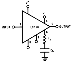 Figure 31. Output Holds at Average of Sampled Input

9.2.6 Increased Slew Current
The slew current can be increased by connecting opposing diodes from the OUTPUT to the HOLD CAPACITOR pins as shown in Figure 32.
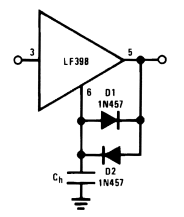 Figure 32. Increased Slew Current
9.2.7 Reset Stabilized Amplifier
The device may be used with LH0042H to create a reset stabilized amplifier with a gain of 1000 as shown in Figure 33.
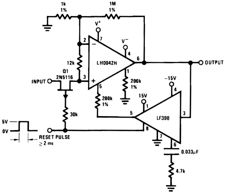
| VOS ≤ 20 µV (No trim) | ZIN ≈ 1 MΩ |


9.2.8 Fast Acquisition, Low Droop Sample and Hold
Two devices may be used along with LM3905 TIMER to create a fast acquisition, low droop sample and hold circuit as shown in Figure 34.
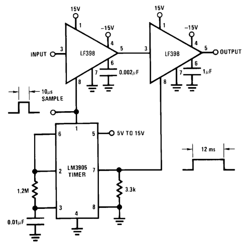 Figure 34. Fast Acquisition, Low Droop Sample and Hold
9.2.9 Synchronous Correlator for Recovering Signals Below Noise Level
The device may be used with two LM122H TIMER devices to create a synchronous correlator for recovering signals below noise level as shown in Figure 35.
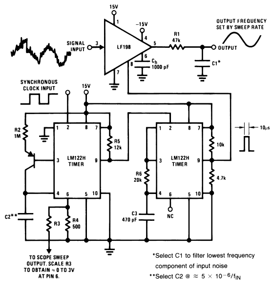 Figure 35. Synchronous Correlator for Recovering Signals Below Noise Level
9.2.10 2-Channel Switch
The HOLD CAPACITOR pin could be alternatively used as a second input to create a 2-channel switch shown Figure 36
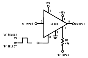 Figure 36. 2-Channel Switch
In the configuration of Figure 36, input signal A and input signal B have the characteristics listed in Table 1.
Table 1. 2-Channel Switch Characteristics
| A | B | |
|---|---|---|
| Gain | 1 ± 0.02% | 1 ± 0.2% |
| ZIN | 1010 Ω | 47 kΩ |
| BW | ≈1 MHz | ≈400 kHz |
| Crosstalk at 1 kHz | –90 dB | –90 dB |
| Offset | ≤ 6 mV | ≤ 75 mV |
9.2.11 DC and AC Zeroing
The device features an OFFSET ADJUST pin which can be connected to a potentiometer to zero the DC offset. Additionally, an inverter may be connected with an AC-coupled potentiometer to the HOLD CAPACITOR pin to create a DC- and AC-zeroing circuit as shown in Figure 37.
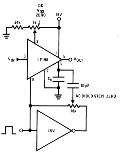 Figure 37. DC and AC Zeroing
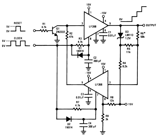
9.2.12 Staircase Generator
The device can be connected as shown in Figure 38 to create a staircase generator.
9.2.13 Differential Hold
Two devices may be connected as shown in Figure 39 to create a differential hold circuit.
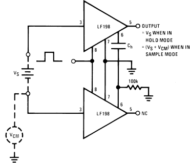 Figure 39. Differential Hold
9.2.14 Capacitor Hysteresis Compensation
The device may be used for capacitor hysteresis compensation as shown in Figure 40.
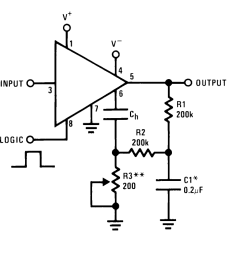
| *Select for time constant C1 = τ/100 kΩ | ||
| **Adjust for amplitude |