JAJSDB3 June 2017 LF298-MIL
PRODUCTION DATA.
- 1 特長
- 2 アプリケーション
- 3 概要
- 4 改訂履歴
- 5 Pin Configuration and Functions
- 6 Specifications
- 7 Parameter Measurement Information
- 8 Detailed Description
-
9 Application and Implementation
- 9.1 Application Information
- 9.2
Typical Applications
- 9.2.1 X1000 Sample and Hold
- 9.2.2 Sample and Difference Circuit
- 9.2.3 Ramp Generator With Variable Reset Level
- 9.2.4 Integrator With Programmable Reset Level
- 9.2.5 Output Holds at Average of Sampled Input
- 9.2.6 Increased Slew Current
- 9.2.7 Reset Stabilized Amplifier
- 9.2.8 Fast Acquisition, Low Droop Sample and Hold
- 9.2.9 Synchronous Correlator for Recovering Signals Below Noise Level
- 9.2.10 2-Channel Switch
- 9.2.11 DC and AC Zeroing
- 9.2.12 Staircase Generator
- 9.2.13 Differential Hold
- 9.2.14 Capacitor Hysteresis Compensation
- 10Power Supply Recommendations
- 11Layout
- 12デバイスおよびドキュメントのサポート
- 13メカニカル、パッケージ、および注文情報
11 Layout
11.1 Layout Guidelines
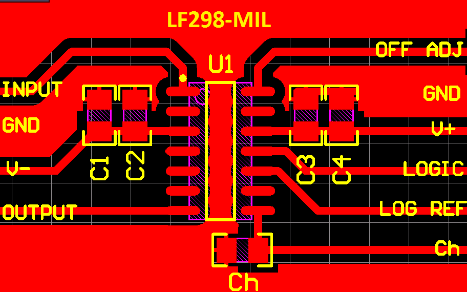
Take care to minimize the loop area formed by the bypass capacitor connection between supply pins and ground. A ground plane underneath the device is recommended; any bypass components to ground should have a nearby via to the ground plane. The optimum bypass capacitor placement is closest to the corresponding supply pin. Use of thicker traces from the bypass capacitors to the corresponding supply pins will lower the power supply inductance and provide a more stable power supply. The feedback components should be placed as close to the device as possible to minimize stray parasitics.
11.2 Layout Example
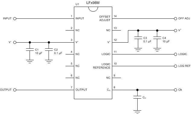
Figure 41 shows an example schematic and layout for the LF298-MIL 8-pin PDIP package.
 Figure 41. Schematic Example
 Figure 42. Layout Example