JAJSDB3 June 2017 LF298-MIL
PRODUCTION DATA.
- 1 特長
- 2 アプリケーション
- 3 概要
- 4 改訂履歴
- 5 Pin Configuration and Functions
- 6 Specifications
- 7 Parameter Measurement Information
- 8 Detailed Description
-
9 Application and Implementation
- 9.1 Application Information
- 9.2
Typical Applications
- 9.2.1 X1000 Sample and Hold
- 9.2.2 Sample and Difference Circuit
- 9.2.3 Ramp Generator With Variable Reset Level
- 9.2.4 Integrator With Programmable Reset Level
- 9.2.5 Output Holds at Average of Sampled Input
- 9.2.6 Increased Slew Current
- 9.2.7 Reset Stabilized Amplifier
- 9.2.8 Fast Acquisition, Low Droop Sample and Hold
- 9.2.9 Synchronous Correlator for Recovering Signals Below Noise Level
- 9.2.10 2-Channel Switch
- 9.2.11 DC and AC Zeroing
- 9.2.12 Staircase Generator
- 9.2.13 Differential Hold
- 9.2.14 Capacitor Hysteresis Compensation
- 10Power Supply Recommendations
- 11Layout
- 12デバイスおよびドキュメントのサポート
- 13メカニカル、パッケージ、および注文情報
6 Specifications
6.1 Absolute Maximum Ratings
over operating free-air temperature range (unless otherwise noted)(1)(2)| MIN | MAX | UNIT | ||
|---|---|---|---|---|
| Supply voltage | ±18 | V | ||
| Power dissipation | (Package limitation, see (3)) | 500 | mW | |
| Operating ambient temperature | –25 | 85 | °C | |
| Input voltage | ±18 | V | ||
| Logic-to-logic reference differential voltage (see (4)) | 7 | −30 | V | |
| Output short circuit duration | Indefinite | |||
| Hold capacitor short circuit duration | 10 | sec | ||
| Lead temperature | H package (soldering, 10 sec.) | 260 | °C | |
| N package (soldering, 10 sec.) | 260 | °C | ||
| M package: vapor phase (60 sec.) | 215 | °C | ||
| Infrared (15 sec.) | 220 | °C | ||
| Storage temperature, Tstg | –65 | 150 | °C | |
(1) Stresses beyond those listed under Absolute Maximum Ratings may cause permanent damage to the device. These are stress ratings only, which do not imply functional operation of the device at these or any other conditions beyond those indicated under Recommended Operating Conditions. Exposure to absolute-maximum-rated conditions for extended periods may affect device reliability.
(2) If Military/Aerospace specified devices are required, please contact the TI Sales Office/ Distributors for availability and specifications.
(3) The maximum power dissipation must be derated at elevated temperatures and is dictated by TJMAX, RθJA, and the ambient temperature, TA. The maximum allowable power dissipation at any temperature is PD = (TJMAX − TA) / RθJA, or the number given in the Absolute Maximum Ratings, whichever is lower. The maximum junction temperature, TJMAX, for the LF298-MIL is 115°C.
(4) Although the differential voltage may not exceed the limits given, the common-mode voltage on the logic pins may be equal to the supply voltages without causing damage to the circuit. For proper logic operation, however, one of the logic pins must always be at least 2 V below the positive supply and 3 V above the negative supply.
6.2 Recommended Operating Conditions
over operating free-air temperature range (unless otherwise noted)| MIN | NOM | MAX | UNIT | |||
|---|---|---|---|---|---|---|
| Supply voltage | ±15 | V | ||||
| TJ | Ambient temperature | –25 | 85 | °C | ||
6.3 Thermal Information
| THERMAL METRIC(1) | LF298-MIL | UNIT | ||
|---|---|---|---|---|
| D (SOIC) | LMC (TO-99) | |||
| 14 PINS | 8 PINS | |||
| RθJA | Junction-to-ambient thermal resistance | 80.6 | 85(2) | °C/W |
| RθJC(top) | Junction-to-case (top) thermal resistance | 38.1 | 20 | °C/W |
| RθJB | Junction-to-board thermal resistance | 35.4 | — | °C/W |
| ψJT | Junction-to-top characterization parameter | 5.8 | — | °C/W |
| ψJB | Junction-to-board characterization parameter | 35.1 | — | °C/W |
(1) For more information about traditional and new thermal metrics, see the Semiconductor and IC Package Thermal Metrics application report.
(2) Board mount in 400 LF/min air flow.
6.4 Electrical Characteristics
The following specifications apply for –VS + 3.5 V ≤ VIN ≤ +VS – 3.5 V, +VS = +15 V, –VS = –15 V, TA = TJ = 25°C, Ch = 0.01 µF, RL = 10 kΩ, LOGIC REFERENCE = 0 V, LOGIC HIGH = 2.5 V, LOGIC LOW = 0 V unless otherwise specified.| PARAMETER | TEST CONDITIONS | MIN | TYP | MAX | UNIT |
|---|---|---|---|---|---|
| Input offset voltage(1) | TJ = 25°C | 1 | 3 | mV | |
| Full temperature range | 5 | mV | |||
| Input bias current(1) | TJ = 25°C | 5 | 25 | nA | |
| Full temperature range | 75 | nA | |||
| Input impedance | TJ = 25°C | 10 | GΩ | ||
| Gain error | TJ = 25°C, RL= 10k | 0.002% | 0.005% | ||
| Full temperature range | 0.02% | ||||
| Feedthrough attenuation ratio at 1 kHz | TJ = 25°C, Ch = 0.01 µF | 86 | 96 | dB | |
| Output impedance | Tj = 25°C, “HOLD” mode | 0.5 | 2 | Ω | |
| Full temperature range | 4 | Ω | |||
| HOLD step(2) | TJ = 25°C, Ch = 0.01 µF, VOUT = 0 | 0.5 | 2 | mV | |
| Supply current(1) | TJ ≥ 25°C | 4.5 | 5.5 | mA | |
| Logic and logic reference input current | TJ = 25°C | 2 | 10 | µA | |
| Leakage current into hold capacitor(1) | TJ = 25°C, hold mode(3) | 30 | 100 | pA | |
| Acquisition time to 0.1% | ΔVOUT = 10 V, Ch = 1000 pF | 4 | µs | ||
| CH = 0.01 µF | 20 | µs | |||
| Hold capacitor charging current | VIN – VOUT = 2 V | 5 | mA | ||
| Supply voltage rejection ratio | VOUT = 0 | 80 | 110 | dB | |
| Differential logic threshold | TJ = 25°C | 0.8 | 1.4 | 2.4 | V |
(1) These parameters ensured over a supply voltage range of ±5 to ±18 V, and an input range of –VS + 3.5 V ≤ VIN ≤ +VS – 3.5 V.
(2) Hold step is sensitive to stray capacitive coupling between input logic signals and the hold capacitor. 1 pF, for instance, will create an additional 0.5-mV step with a 5-V logic swing and a 0.01-µF hold capacitor. Magnitude of the hold step is inversely proportional to hold capacitor value.
(3) Leakage current is measured at a junction temperature of 25°C. The effects of junction temperature rise due to power dissipation or elevated ambient can be calculated by doubling the 25°C value for each 11°C increase in chip temperature. Leakage is guaranteed over full input signal range.
6.5 Typical Characteristics
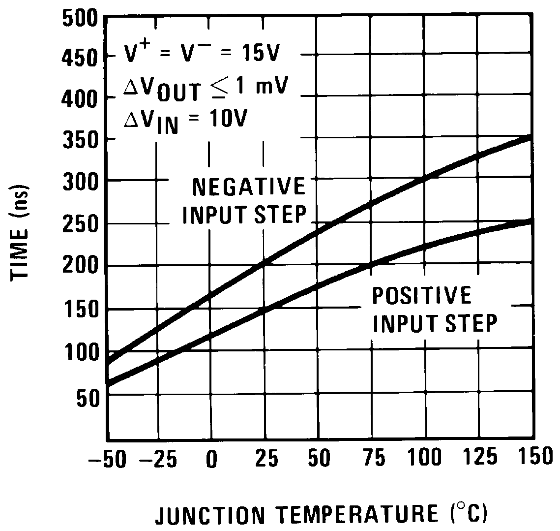 Figure 1. Aperture Time
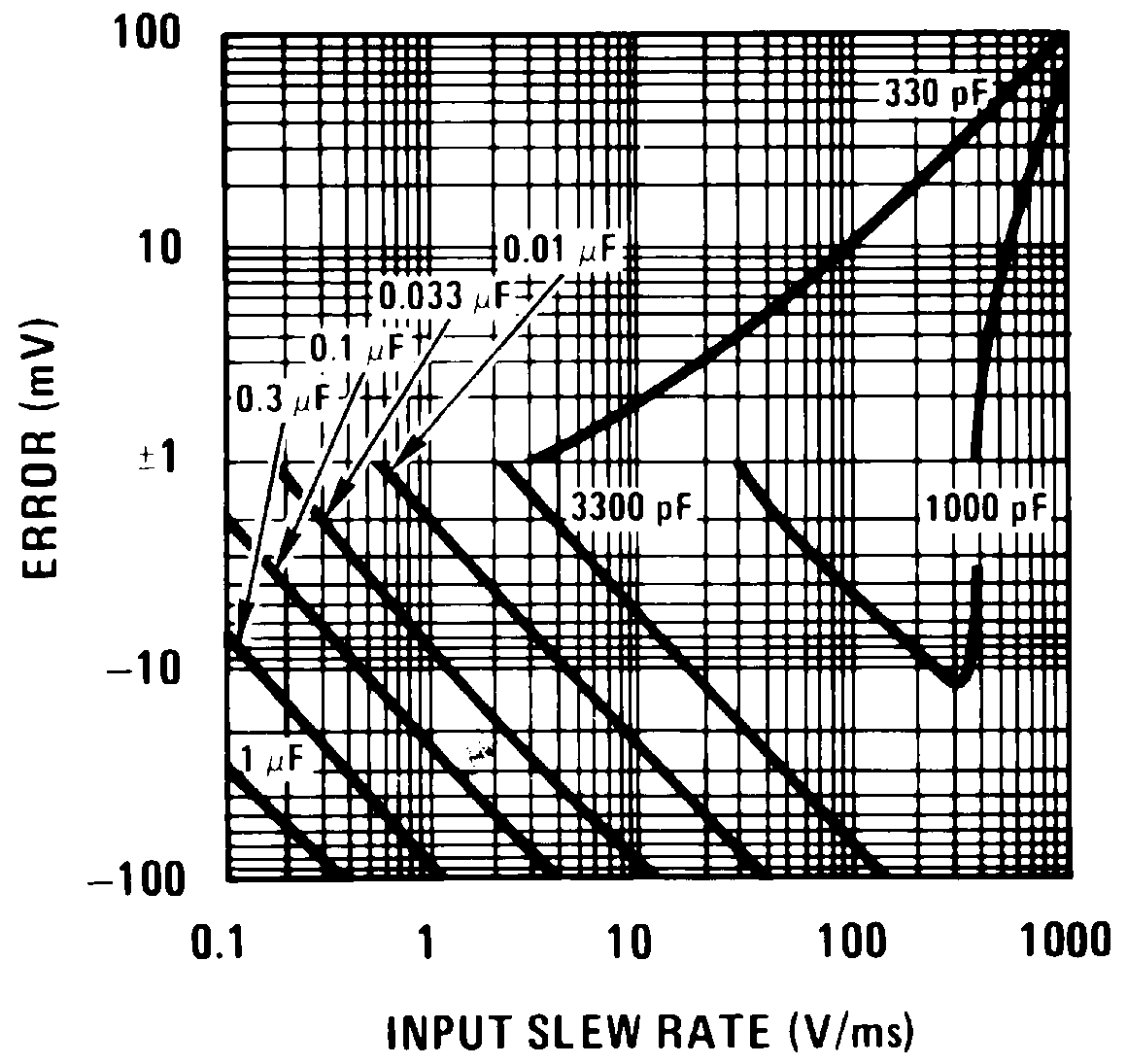 Figure 3. Dynamic Sampling Error
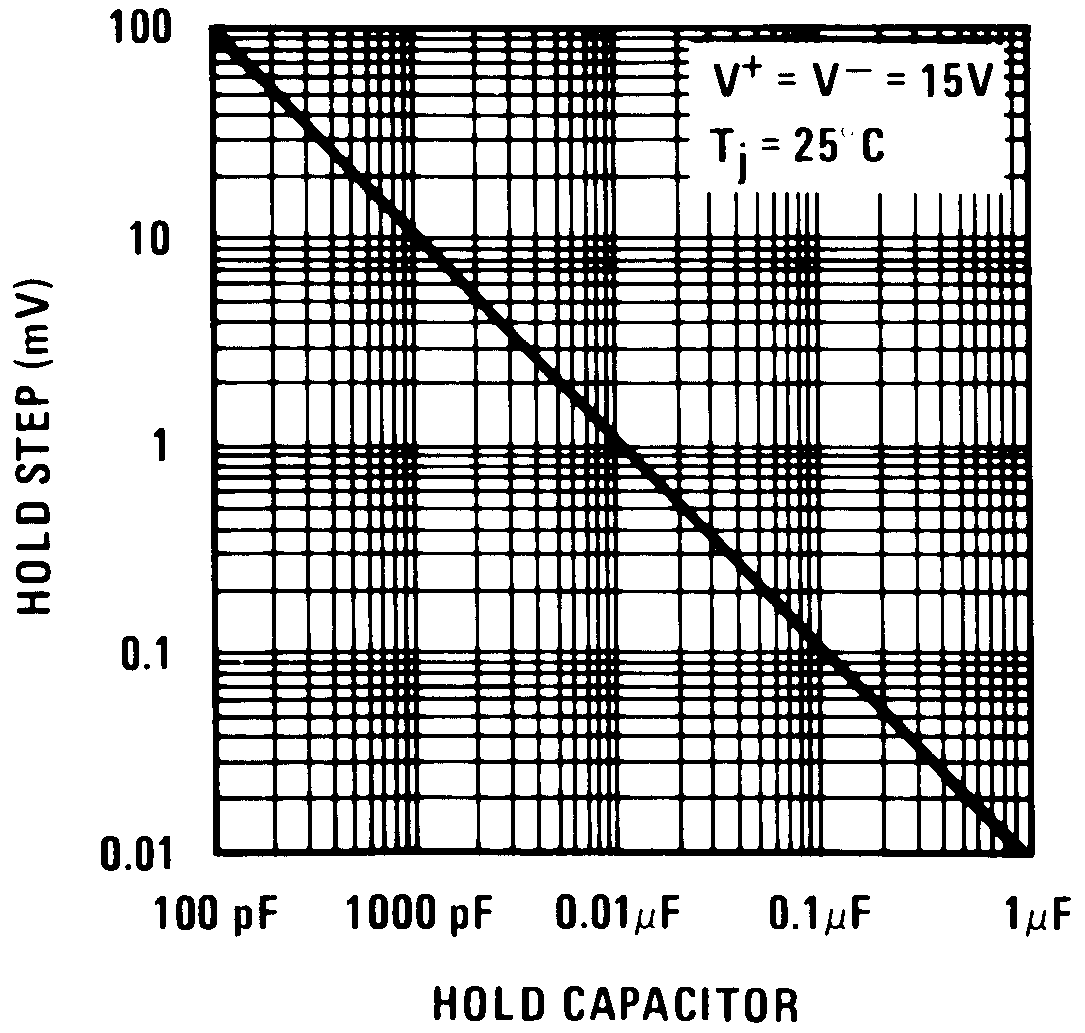 Figure 5. Hold Step
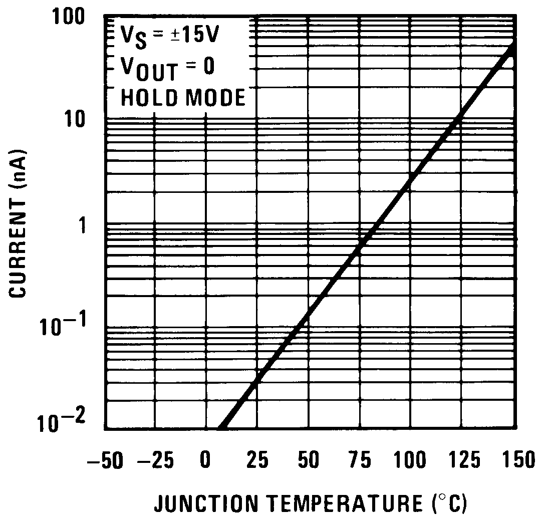 Figure 7. Leakage Current into Hold Capacitor
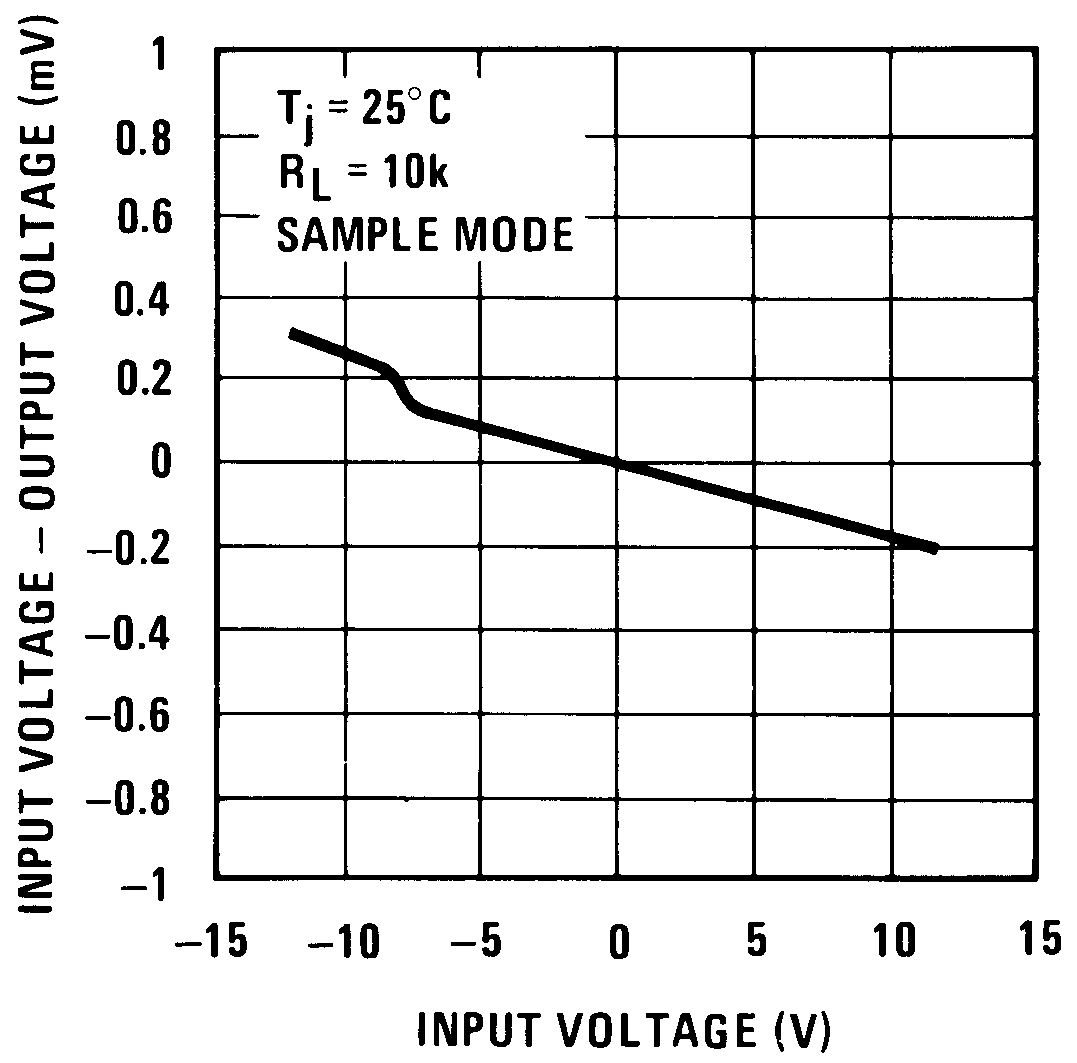 Figure 9. Gain Error
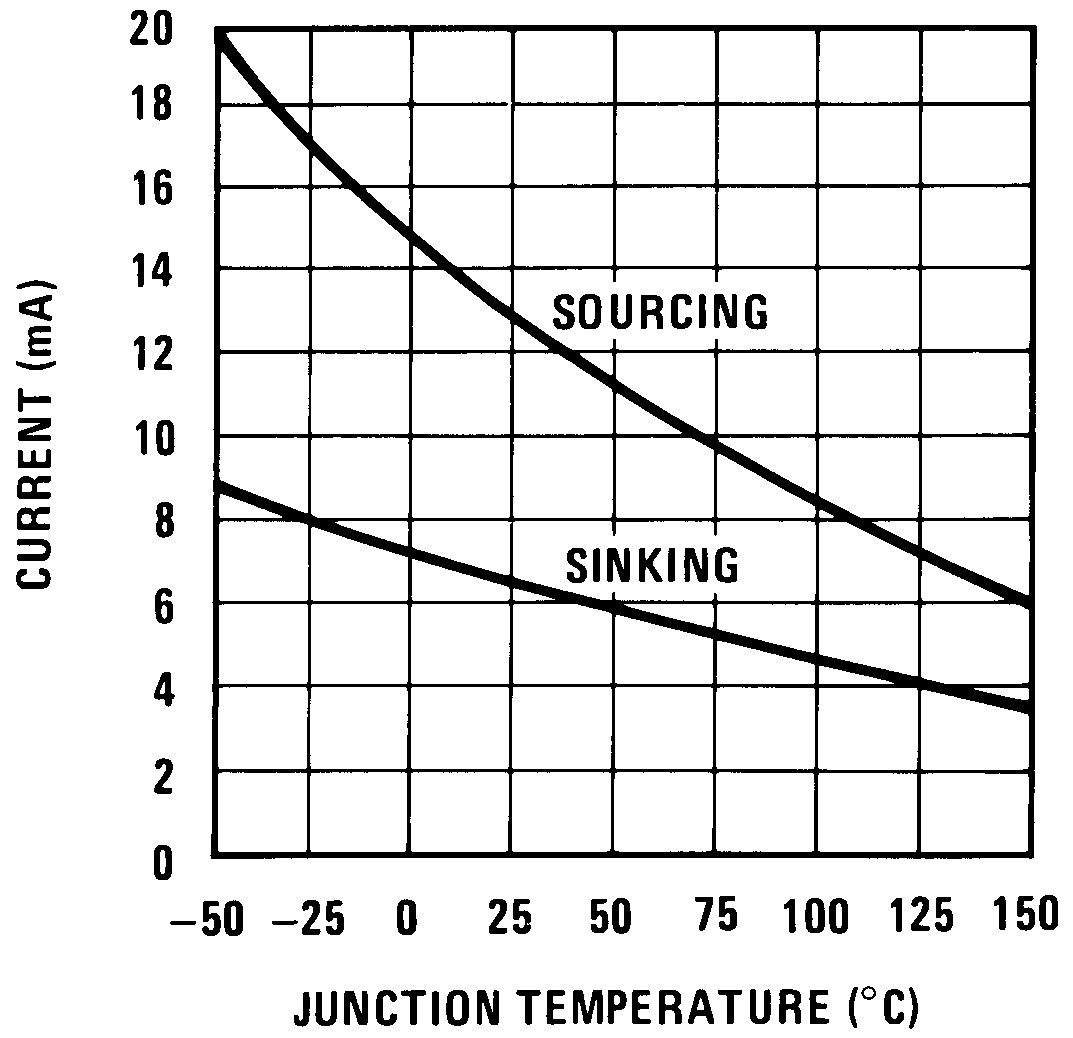 Figure 11. Output Short-Circuit Current
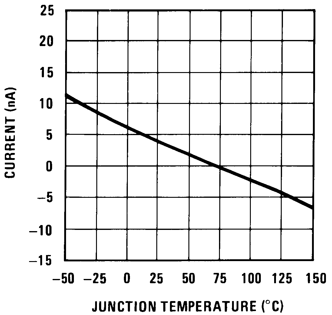 Figure 13. Input Bias Current
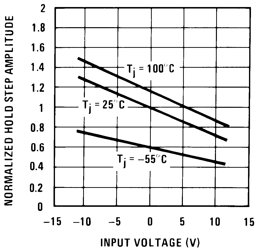 Figure 15. Hold Step vs Input Voltage
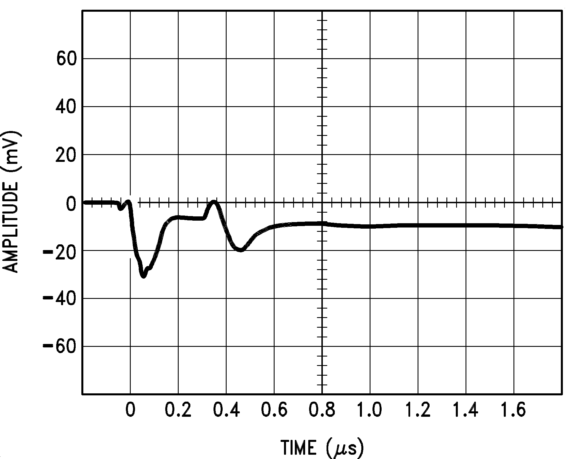 Figure 17. Output Transient at Start of Hold Mode
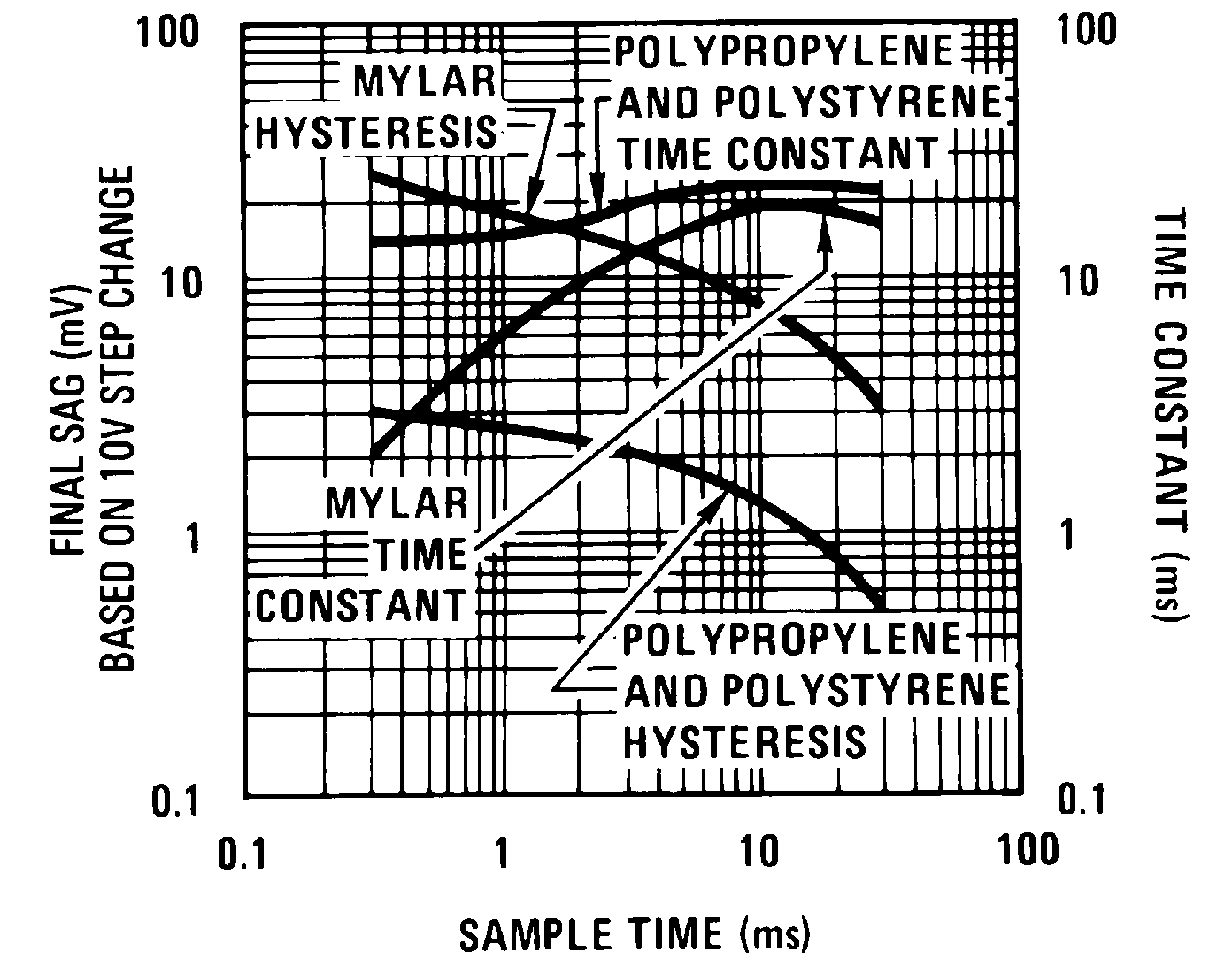 Figure 2. Dielectric Absorption Error in Hold Capacitor
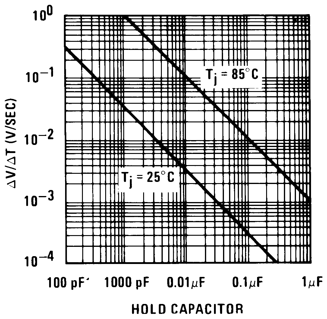 Figure 4. Output Droop Rate
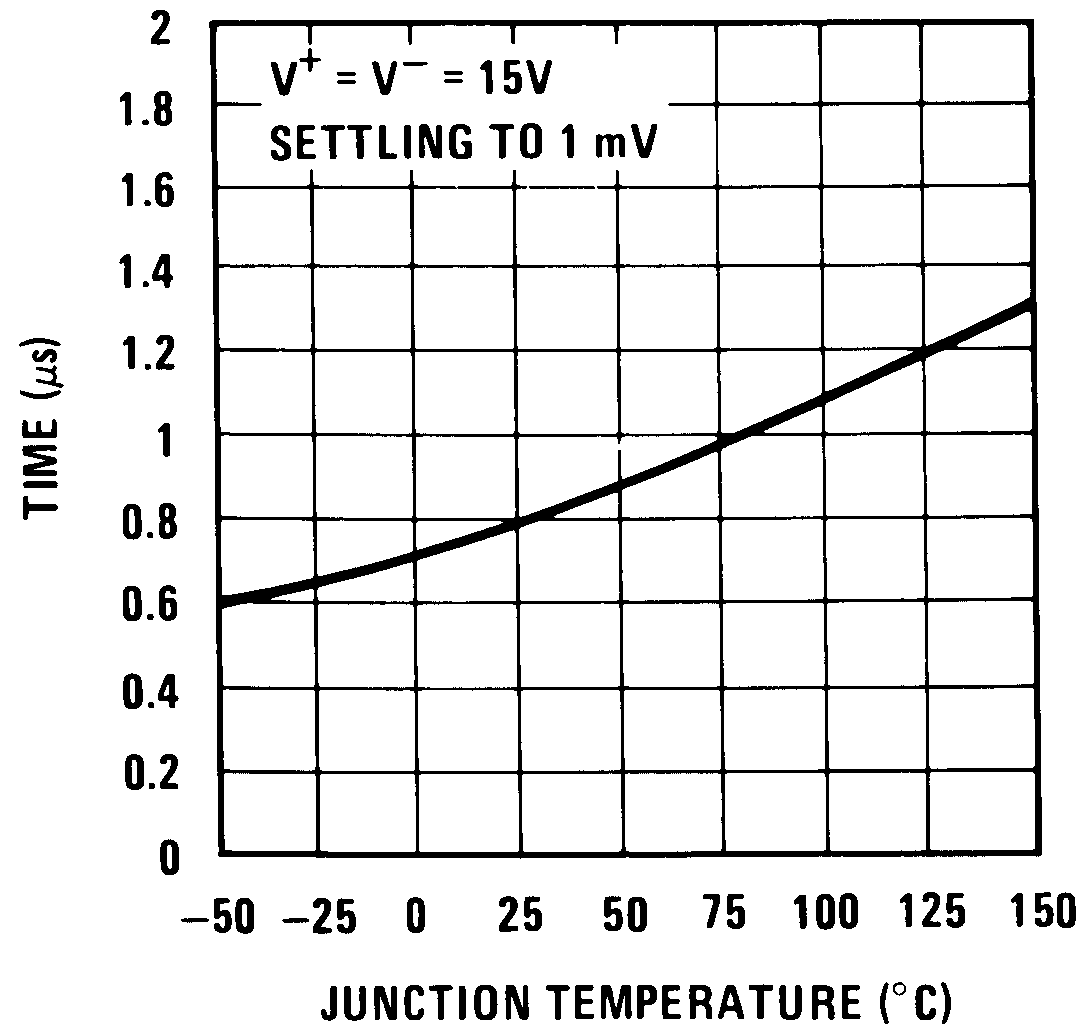 Figure 6. Hold Settling Time
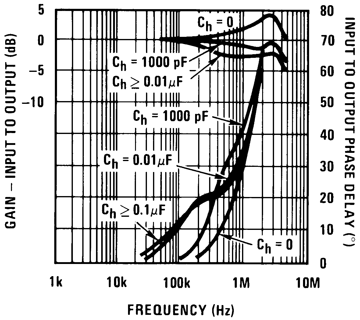 Figure 8. Phase and Gain (Input to Output, Small Signal)
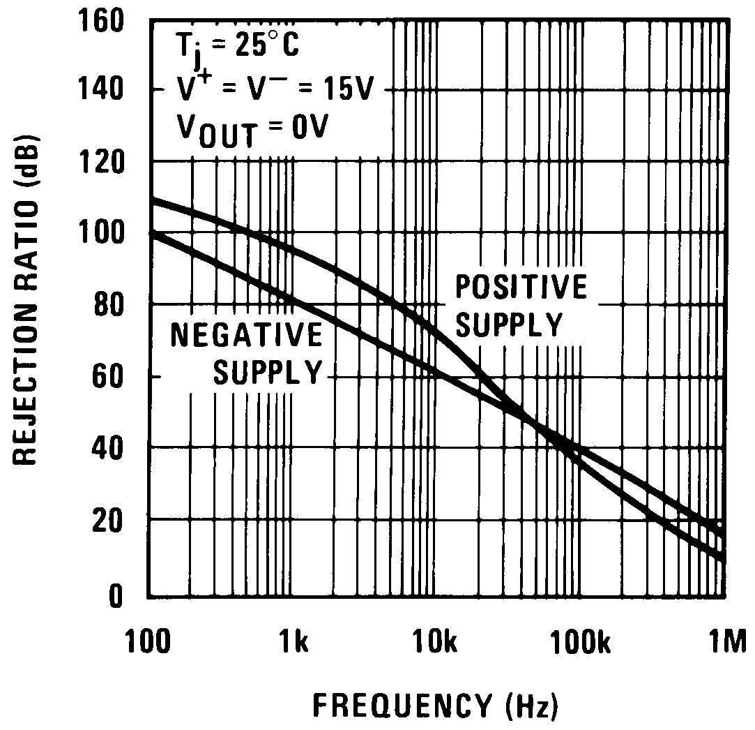 Figure 10. Power Supply Rejection
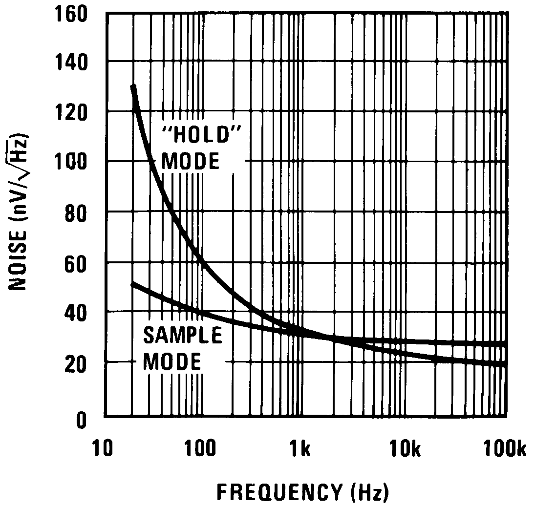 Figure 12. Output Noise
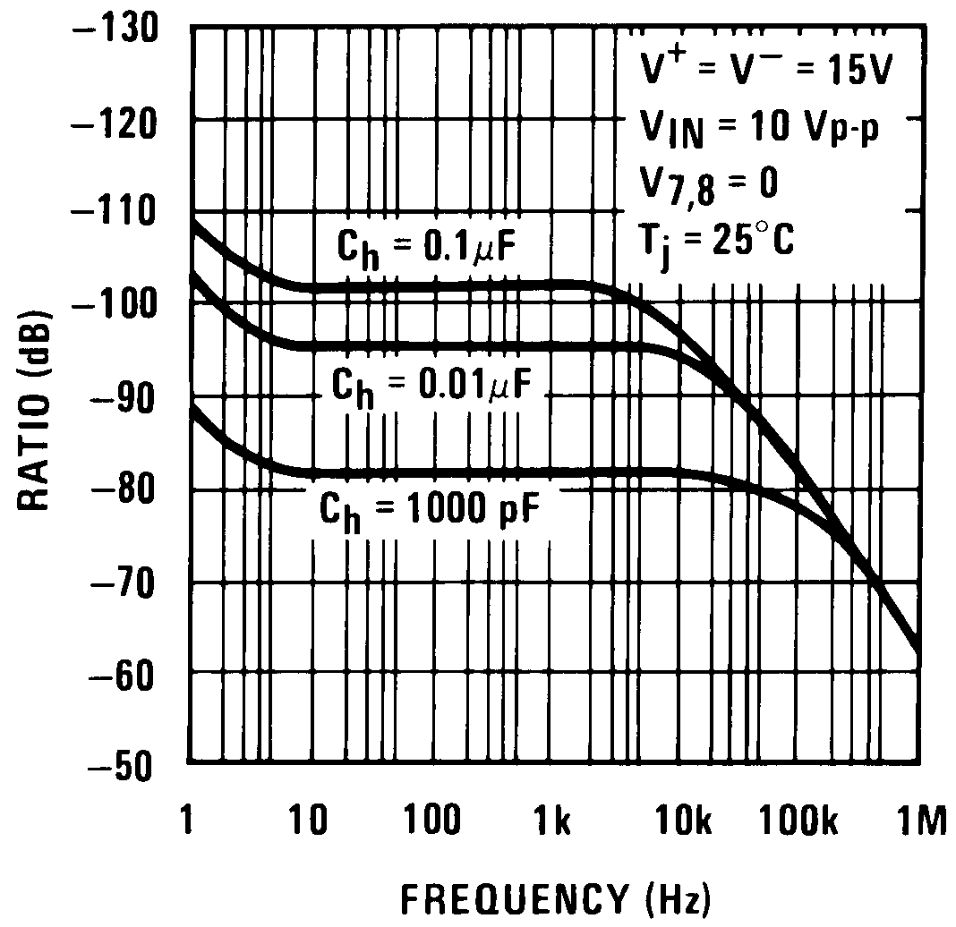 Figure 14. Feedthrough Rejection Ratio (Hold Mode)
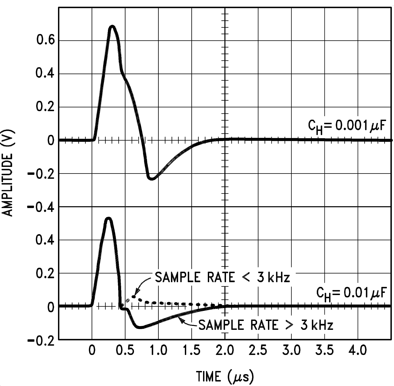 Figure 16. Output Transient at Start of Sample Mode