JAJSDB3 June 2017 LF298-MIL
PRODUCTION DATA.
- 1 特長
- 2 アプリケーション
- 3 概要
- 4 改訂履歴
- 5 Pin Configuration and Functions
- 6 Specifications
- 7 Parameter Measurement Information
- 8 Detailed Description
-
9 Application and Implementation
- 9.1 Application Information
- 9.2
Typical Applications
- 9.2.1 X1000 Sample and Hold
- 9.2.2 Sample and Difference Circuit
- 9.2.3 Ramp Generator With Variable Reset Level
- 9.2.4 Integrator With Programmable Reset Level
- 9.2.5 Output Holds at Average of Sampled Input
- 9.2.6 Increased Slew Current
- 9.2.7 Reset Stabilized Amplifier
- 9.2.8 Fast Acquisition, Low Droop Sample and Hold
- 9.2.9 Synchronous Correlator for Recovering Signals Below Noise Level
- 9.2.10 2-Channel Switch
- 9.2.11 DC and AC Zeroing
- 9.2.12 Staircase Generator
- 9.2.13 Differential Hold
- 9.2.14 Capacitor Hysteresis Compensation
- 10Power Supply Recommendations
- 11Layout
- 12デバイスおよびドキュメントのサポート
- 13メカニカル、パッケージ、および注文情報
8 Detailed Description
8.1 Overview
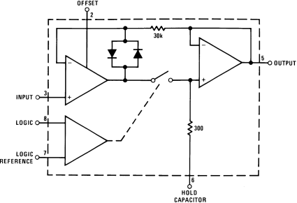
The LF298-MIL device is a monolithic sample-and-hold circuit that uses BI-FET technology to obtain ultrahigh DC accuracy with fast acquisition of signal and low droop rate. Operating as a unity-gain follower, DC gain accuracy is 0.002% typical and acquisition time is as low as 6 µs to 0.01%. A bipolar input stage is used to achieve low offset voltage and wide bandwidth. Input offset adjust is accomplished with a single pin, and does not degrade input offset drift. Input impedance of 1010 Ω allows high-source impedances to be used without degrading accuracy.
8.2 Functional Block Diagram

8.3 Feature Description
The LF298-MIL OUTPUT tracks the INPUT signal by charging and discharging the hold capacitor. The OUTPUT can be held at any given time by pulling the LOGIC input low relative to the LOGIC REFERENCE voltage and resume sampling when LOGIC returns high. Additionally, the OFFSET pin can be used to zero the offset voltage present at the INPUT.
8.4 Device Functional Modes
The LF298-MIL device has a sample mode and hold mode controlled by the LOGIC voltage relative to the LOGIC REFERENCE voltage. The device is in sample mode when the LOGIC input is pulled high relative to the LOGIC REFERENCE voltage and in hold mode when the LOGIC input is pulled low relative to the LOGIC REFERENCE. In sample mode, the output is tracking the input signal by charging and discharging the hold capacitor. Smaller values of hold capacitance will allow the output to track faster signals. In hold mode the input signal is disconnected from the signal path and the output retains the value on the hold capacitor. Larger values of capacitance will have a smaller droop rate as shown in Figure 4.