JAJSDB2 June 2017 LF356-MIL
PRODUCTION DATA.
- 1 特長
- 2 アプリケーション
- 3 概要
- 4 改訂履歴
- 5 Pin Configuration and Functions
-
6 Specifications
- 6.1 Absolute Maximum Ratings
- 6.2 ESD Ratings
- 6.3 Recommended Operating Conditions
- 6.4 Thermal Information
- 6.5 AC Electrical Characteristics, TA = TJ = 25°C, VS = ±15 V
- 6.6 DC Electrical Characteristics, TA = TJ = 25°C, VS = ±15 V
- 6.7 DC Electrical Characteristics
- 6.8 Power Dissipation Ratings
- 6.9 Typical Characteristics
- 7 Detailed Description
- 8 Application and Implementation
- 9 Power Supply Recommendations
- 10Layout
- 11デバイスおよびドキュメントのサポート
- 12メカニカル、パッケージ、および注文情報
8 Application and Implementation
NOTE
Information in the following applications sections is not part of the TI component specification, and TI does not warrant its accuracy or completeness. TI’s customers are responsible for determining suitability of components for their purposes. Customers should validate and test their design implementation to confirm system functionality.
8.1 Application Information
These are op amps with JFET input devices. These JFETs have large reverse breakdown voltages from gate to source and drain eliminating the need for clamps across the inputs. Therefore large differential input voltages can easily be accommodated without a large increase in input current. The maximum differential input voltage is independent of the supply voltages. However, neither of the input voltages should be allowed to exceed the negative supply as this will cause large currents to flow which can result in a destroyed unit.
Exceeding the negative common-mode limit on either input will force the output to a high state, potentially causing a reversal of phase to the output. Exceeding the negative common-mode limit on both inputs will force the amplifier output to a high state. In neither case does a latch occur since raising the input back within the common-mode range again puts the input stage and thus the amplifier in a normal operating mode.
Exceeding the positive common-mode limit on a single input will not change the phase of the output however, if both inputs exceed the limit, the output of the amplifier will be forced to a high state.
These amplifiers will operate with the common-mode input voltage equal to the positive supply. In fact, the common-mode voltage can exceed the positive supply by approximately 100 mV independent of supply voltage and over the full operating temperature range. The positive supply can therefore be used as a reference on an input as, for example, in a supply current monitor and/or limiter.
Precautions should be taken to ensure that the power supply for the integrated circuit never becomes reversed in polarity or that the unit is not inadvertently installed backwards in a socket as an unlimited current surge through the resulting forward diode within the IC could cause fusing of the internal conductors and result in a destroyed unit.
All of the bias currents in these amplifiers are set by FET current sources. The drain currents for the amplifiers are therefore essentially independent of supply voltage.
As with most amplifiers, care should be taken with lead dress, component placement and supply decoupling in order to ensure stability. For example, resistors from the output to an input should be placed with the body close to the input to minimize pick-up and maximize the frequency of the feedback pole by minimizing the capacitance from the input to ground.
A feedback pole is created when the feedback around any amplifier is resistive. The parallel resistance and capacitance from the input of the device (usually the inverting input) to AC ground set the frequency of the pole. In many instances the frequency of this pole is much greater than the expected 3-dB frequency of the closed loop gain and consequently there is negligible effect on stability margin. However, if the feedback pole is less than approximately six times the expected 3-dB frequency a lead capacitor should be placed from the output to the input of the op amp. The value of the added capacitor should be such that the RC time constant of this capacitor and the resistance it parallels is greater than or equal to the original feedback pole time constant.
8.2 Typical Application
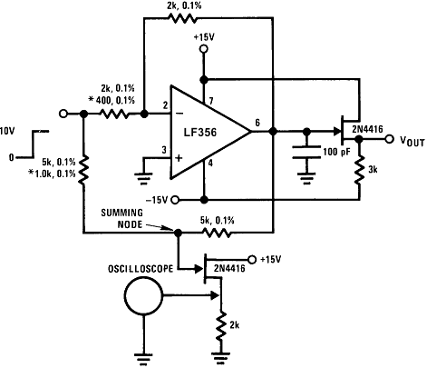 Figure 23. Settling Time Test Circuit
8.2.1 Design Requirements
Settling time is tested with the LF35x connected as unity gain inverter and LF357 connected for AV = −5
8.2.2 Detailed Design Procedure
Connect the circuit components as shown in Figure 23. In particular, use FET to isolate the probe capacitance.
Apply a 10-V step function to the input.
Use an oscilloscope to probe the circuit as shown in Figure 23.
8.2.3 Application Curve
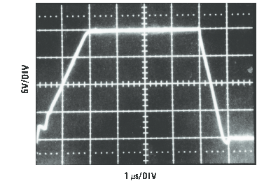 Figure 24. Large Signal Inverter Output, VOUT (from Settling Time Circuit)
8.3 System Examples
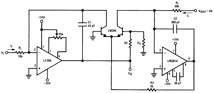 Figure 25. Fast Logarithmic Converter
- Dynamic range: 100 μA ≤ Ii ≤ 1 mA (5 decades), |VO| = 1 V/decade
- Transient response: 3 μs for ΔIi = 1 decade
- C1, C2, R2, R3: added dynamic compensation
- VOS adjust the LF156 to minimize quiescent error
- RT: Tel Labs type Q81 + 0.3%/°C

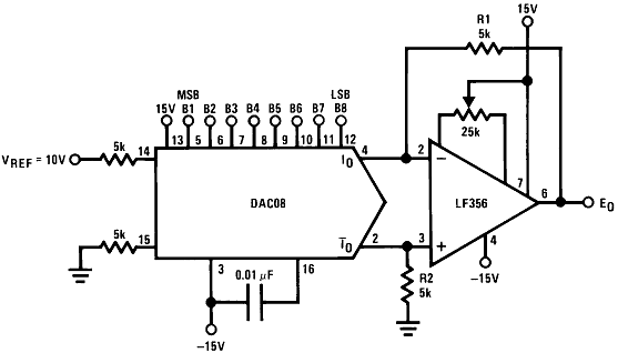 Figure 26. 8-Bit D/A Converter With Symmetrical Offset Binary Operation
- R1, R2 should be matched within ±0.05%
- Full-scale response time: 3 μs
Table 1. Bit Illustration of the 8-Bit D/A Converter
| EO | B1 | B2 | B3 | B4 | B5 | B6 | B7 | B8 | COMMENTS |
|---|---|---|---|---|---|---|---|---|---|
| +9.920 | 1 | 1 | 1 | 1 | 1 | 1 | 1 | 1 | Positive Full-Scale |
| +0.040 | 1 | 0 | 0 | 0 | 0 | 0 | 0 | 0 | (+) Zero-Scale |
| −0.040 | 0 | 1 | 1 | 1 | 1 | 1 | 1 | 1 | (−) Zero-Scale |
| −9.920 | 0 | 0 | 0 | 0 | 0 | 0 | 0 | 0 | Negative Full-Scale |
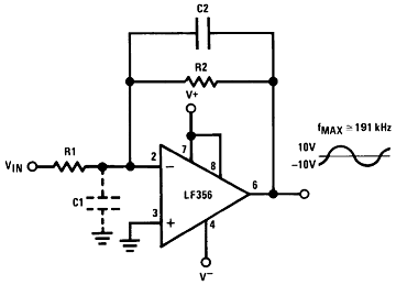 Figure 27. Wide BW Low Noise, Low Drift Amplifier

Parasitic input capacitance C1 ≃ (3 pF for LF155, LF156 and LF357 plus any additional layout capacitance) interacts with feedback elements and creates undesirable high frequency pole. To compensate add C2 such that: R2 C2 ≃ R1 C1.
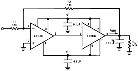 Figure 28. Boosting the LF156 With a Current Amplifier
- IOUT(MAX) ≃ 150 mA (will drive RL ≥ 100 Ω)
- No additional phase shift added by the current amplifier

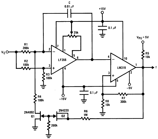 Figure 29. Decades VCO
R1, R4 matched. Linearity 0.1% over 2 decades.

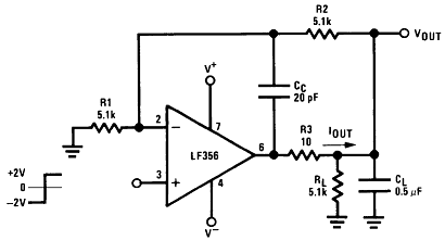 Figure 30. Isolating Large Capacitive Loads
- Overshoot 6%
- ts 10 μs
- When driving large CL, the VOUT slew rate determined by CL and IOUT(MAX):

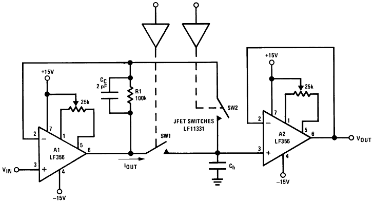 Figure 31. Fast Sample and Hold
- Both amplifiers (A1, A2) have feedback loops individually closed with stable responses (overshoot negligible)
- Acquisition time TA, estimated by:
- LF156 develops full Sr output capability for VIN ≥ 1 V
- Addition of SW2 improves accuracy by putting the voltage drop across SW1 inside the feedback loop
- Overall accuracy of system determined by the accuracy of both amplifiers, A1 and A2
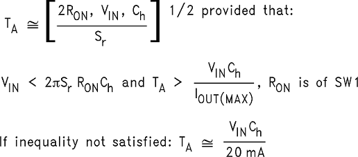
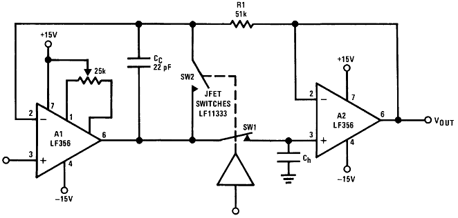 Figure 32. High Accuracy Sample and Hold
- By closing the loop through A2, the VOUT accuracy will be determined uniquely by A1.
- No VOS adjust required for A2.
- TA can be estimated by same considerations as previously but, because of the added
- propagation delay in the feedback loop (A2) the overshoot is not negligible.
- Overall system slower than fast sample and hold
- R1, CC: additional compensation
- Use LF156 for
- Fast settling time
- Low VOS
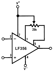 Figure 33. VOS Adjustment
- VOS is adjusted with a 25-k potentiometer
- The potentiometer wiper is connected to V+
- For potentiometers with temperature coefficient of 100 ppm/°C or less the additional drift with adjust
is ≈ 0.5 μV/°C/mV of adjustment - Typical overall drift: 5 μV/°C ±(0.5 μV/°C/mV of adj.)
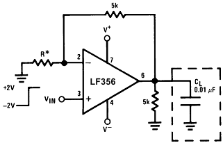 Figure 34. Driving Capacitive Loads
- *LF15x R = 5k, LF357 R = 1.25 k
- Due to a unique output stage design, these amplifiers have the ability to drive large capacitive loads and still maintain stability. CL(MAX) ≃ 0.01 μF.
- Overshoot ≤ 20%, Settling time (ts) ≃ 5 μs