SNOSBH4E May 1998 – October 2015 LM10
PRODUCTION DATA.
- 1 Features
- 2 Applications
- 3 Description
- 4 Revision History
- 5 Pin Configuration and Functions
- 6 Specifications
- 7 Detailed Description
- 8 Application and Implementation
- 9 Power Supply Recommendations
- 10Layout
- 11Device and Documentation Support
- 12Mechanical, Packaging, and Orderable Information
6 Specifications
6.1 Absolute Maximum Ratings
See (5)(1)(6)| MIN | MAX | UNIT | |||
|---|---|---|---|---|---|
| Total supply voltage | LM10/LM10B/LM10C | 45 | V | ||
| LM10BL/LM10CL | 7 | V | |||
| Differential input voltage(2) | LM10/LM10B/LM10C | ±40 | V | ||
| LM10BL/LM10CL | ±7 | V | |||
| Power dissipation(3) | Internally limited | ||||
| Output short-circuit duration(4) | Continuous | ||||
| Lead temperature | TO | Soldering (10 seconds) | 300 | °C | |
| DIP | Soldering (10 seconds) | 260 | °C | ||
| Vapor phase (60 seconds) | 215 | °C | |||
| Infrared (15 seconds) | 220 | °C | |||
| Maximum junction temperature | LM10 | 150 | °C | ||
| LM10B | 100 | °C | |||
| LM10C | 85 | °C | |||
| Storage temperature, Tstg | −55 | 150 | °C | ||
(1) Stresses beyond those listed under Absolute Maximum Ratings may cause permanent damage to the device. These are stress ratings only, and functional operation of the device at these or any other conditions beyond those indicated under Recommended Operating Conditions is not implied. Exposure to absolute-maximum-rated conditions for extended periods may affect device reliability.
(2) The Input voltage can exceed the supply voltages provided that the voltage from the input to any other terminal does not exceed the maximum differential input voltage and excess dissipation is accounted for when VIN < V−.
(3) The maximum, operating-junction temperature is 150°C for the LM10, 100°C for the LM10B(L) and 85°C for the LM10C(L). At elevated temperatures, devices must be derated based on package thermal resistance.
(4) Internal thermal limiting prevents excessive heating that could result in sudden failure, but the IC can be subjected to accelerated stress with a shorted output and worst-case conditions.
(5) Refer to RETS10X for LM10H military specifications.
(6) If Military/Aerospace specified devices are required, please contact the TI Sales Office/Distributors for availability and specifications.
6.2 Recommended Operating Conditions
over operating free-air temperature range (unless otherwise noted)| MIN | NOM | MAX | UNIT | ||
|---|---|---|---|---|---|
| VS | Supply input voltage range (V–) – (V+) | 1.2 | 40 | V | |
| VCM | Common-mode voltage | (V–) | (V+) – 0.85 | V | |
| VREF | Reference voltage | 0.2 | V | ||
| IREF | Reference current | 0 | 1 | mA | |
6.3 Thermal Information
| THERMAL METRIC(1) | LM10 | UNIT | |||
|---|---|---|---|---|---|
| NEV (SDIP) | NPA (SOIC) | P (PDIP) | |||
| 8 PINS | 14 PINS | 8 PINS | |||
| RθJA | Junction-to-ambient thermal resistance | 150 | 90 | 87 | °C/W |
| RθJC(top) | Junction-to-case (top) thermal resistance | 45 | — | — | °C/W |
(1) For more information about traditional and new thermal metrics, see the Semiconductor and IC Package Thermal Metrics application report, SPRA953.
6.4 Electrical Characteristics LM10/LM10B
TJ=25°C unless otherwise specified(1)| PARAMETER | TEST CONDITIONS | MIN | TYP | MAX | UNIT | |
|---|---|---|---|---|---|---|
| Input offset voltage | TJ=25°C | 0.3 | 2 | mV | ||
| TMIN ≤ TJ ≤ TMAX (see (1)) | 3 | mV | ||||
| Input offset current(2) | TJ=25°C | 0.25 | 0.7 | nA | ||
| TMIN ≤ TJ ≤ TMAX (see (1)) | 1.5 | nA | ||||
| Input bias current | TJ=25°C | 10 | 20 | nA | ||
| TMIN ≤ TJ ≤ TMAX (see (1)) | 30 | nA | ||||
| Input resistance | TJ=25°C | 250 | 500 | kΩ | ||
| TMIN ≤ TJ ≤ TMAX (see (1)) | 150 | kΩ | ||||
| Large signal voltage gain | VS = ±20 V, IOUT = 0 | 120 | 400 | V/mV | ||
| VOUT = ±19.95 V, TMIN ≤ TJ ≤ TMAX (see (1)) | 80 | V/mV | ||||
| VS = ±20 V, VOUT = ±19.4 V | 50 | 130 | V/mV | |||
| IOUT = ±20 mA, TMIN ≤ TJ ≤ TMAX (see (1)) | 20 | V/mV | ||||
| IOUT = ±15 mA, TMIN ≤ TJ ≤ TMAX (see (1)) | 20 | V/mV | ||||
| VS = ±0.6 V, IOUT = ±2 mA | 1.5 | 3 | V/mV | |||
| VS = ±0.65 V, IOUT = ±2 mA, TMIN ≤ TJ ≤ TMAX (see (1)) | 1.5 | 3 | V/mV | |||
| VOUT = ±0.4 V, TMIN ≤ TJ ≤ TMAX (see (1)) | 0.5 | V/mV | ||||
| VOUT = ±0.3 V, VCM = −0.4 V, TMIN ≤ TJ ≤ TMAX (see (1)) | 0.5 | V/mV | ||||
| Shunt gain(3) | 1.2 V ≤ VOUT ≤ 40 V, RL = 1.1 kΩ | 14 | 33 | V/mV | ||
| 1.3 V ≤ VOUT ≤ 40 V, RL = 1.1 kΩ, TMIN ≤ TJ ≤ TMAX (see (1)) | 14 | 33 | V/mV | |||
| 0.1 mA ≤ IOUT ≤ 5 mA, TMIN ≤ TJ ≤ TMAX (see (1)) | 6 | V/mV | ||||
| 1.5 V ≤ V+ ≤ 40 V, RL = 250 Ω | 8 | 25 | V/mV | |||
| 0.1 mA ≤ IOUT ≤ 20 mA, TMIN ≤ TJ ≤ TMAX (see (1)) | 4 | V/mV | ||||
| Common-mode rejection | −20 V ≤ VCM ≤ 19.15 V | 93 | 102 | dB | ||
| −20 V ≤ VCM ≤ 19 V, TMIN ≤ TJ ≤ TMAX (see (1)) | 93 | 102 | dB | |||
| VS = ±20 V, TMIN ≤ TJ ≤ TMAX (see (1)) | 87 | dB | ||||
| Supply-voltage rejection | −0.2 V ≥ V− ≥ −39 V | 90 | 96 | dB | ||
| V+ = 1 V, TMIN ≤ TJ ≤ TMAX (see (1)) | 84 | dB | ||||
| V+ = 1.1 V, TMIN ≤ TJ ≤ TMAX (see (1)) | 84 | dB | ||||
| 1 V ≤ V+ ≤ 39.8 V | 96 | 106 | dB | |||
| 1.1 V ≤ V+ ≤ 39.8 V, TMIN ≤ TJ ≤ TMAX (see (1)) | 96 | 106 | dB | |||
| V− = −0.2 V, TMIN ≤ TJ ≤ TMAX (see (1)) | 90 | dB | ||||
| Offset voltage drift | 2 | μV/°C | ||||
| Offset current drift | 2 | pA/°C | ||||
| Bias current drift | TC < 100°C | 60 | pA/°C | |||
| Line regulation | 1.2 V ≤ VS ≤ 40 V | 0.001 | 0.003 | %/V | ||
| 1.3 V ≤ VS ≤ 40 V, TMIN ≤ TJ ≤ TMAX (see (1)) | 0.001 | 0.003 | %/V | |||
| 0 ≤ IREF ≤ 1 mA, VREF = 200 mV, TMIN ≤ TJ ≤ TMAX (see (1)) | 0.006 | %/V | ||||
| Load regulation | 0 ≤ IREF ≤ 1 mA | 0.01% | 0.1% | |||
| V+− VREF ≥ 1 V, TMIN ≤ TJ ≤ TMAX (see (1)) | 0.15% | |||||
| V+− VREF ≥ 1.1 V, TMIN ≤ TJ ≤ TMAX (see (1)) | 0.15% | |||||
| Amplifier gain | 0.2 V ≤ VREF ≤ 35 V | TJ=25°C | 50 | 75 | V/mV | |
| TMIN ≤ TJ ≤ TMAX (see (1)) | 23 | V/mV | ||||
| Feedback sense voltage | TJ=25°C | 195 | 200 | 205 | mV | |
| TMIN ≤ TJ ≤ TMAX (see (1)) | 194 | 206 | mV | |||
| Feedback current | TJ=25°C | 20 | 50 | nA | ||
| TMIN ≤ TJ ≤ TMAX (see (1)) | 65 | nA | ||||
| Reference drift | 0.002 | %/°C | ||||
| Supply current | TJ=25°C | 270 | 400 | μA | ||
| TMIN ≤ TJ ≤ TMAX (see (1)) | 500 | μA | ||||
| Supply current change | 1.2 V ≤ VS ≤ 40 V | TJ=25°C | 15 | μA | ||
| TMIN ≤ TJ ≤ TMAX (see (1)) | 75 | |||||
| 1.3 V ≤ VS ≤ 40 V | TJ=25°C | 15 | μA | |||
| TMIN ≤ TJ ≤ TMAX (see (1)) | 75 | |||||
(1) These specifications apply for V− ≤ VCM ≤ V+− 0.85 V, 1 V (TMIN ≤ TJ ≤ TMAX), 1.2 V, 1.3 V (TMIN ≤ TJ ≤ TMAX) < VS ≤ VMAX, VREF = 0.2 V and 0 ≤ IREF ≤ 1 mA, unless otherwise specified: VMAX = 40 V for the standard part and 6.5 V for the low voltage part. The full-temperature-range operation is −55°C to 125°C for the LM10, −25°C to 85°C for the LM10B(L) and 0°C to 70°C for the LM10C(L). The specifications do not include the effects of thermal gradients (τ1 ≃ 20 ms), die heating (τ2 ≃ 0.2 s) or package heating. Gradient effects are small and tend to offset the electrical error (see curves).
(2) For TJ > 90°C, IOS may exceed 1.5 nA for VCM = V−. With TJ = 125°C and V− ≤ VCM ≤ V− + 0.1 V, IOS ≤ 5 nA.
(3) This defines operation in floating applications such as the bootstrapped regulator or two-wire transmitter. Output is connected to the V+ terminal of the IC and input common mode is referred to V− (see System Examples). Effect of larger output-voltage swings with higher load resistance can be accounted for by adding the positive-supply rejection error.
6.5 Electrical Characteristics, LM10C
TJ=25°C unless otherwise specified(1)| PARAMETER | TEST CONDITIONS | MIN | TYP | MAX | UNIT | |
|---|---|---|---|---|---|---|
| Input offset voltage | TJ=25°C | 0.5 | 4 | mV | ||
| TMIN ≤ TJ ≤ TMAX (see (1)) | 5 | mV | ||||
| Input offset current(2) | TJ=25°C | 0.4 | 2 | nA | ||
| TMIN ≤ TJ ≤ TMAX (see (1)) | 3 | nA | ||||
| Input bias current | TJ=25°C | 12 | 30 | nA | ||
| TMIN ≤ TJ ≤ TMAX (see (1)) | 40 | nA | ||||
| Input resistance | TJ=25°C | 150 | 400 | kΩ | ||
| TMIN ≤ TJ ≤ TMAX (see (1)) | 115 | kΩ | ||||
| Large signal voltage gain | VS = ±20 V, IOUT = 0 | 80 | 400 | V/mV | ||
| VOUT = ±19.95 V, TMIN ≤ TJ ≤ TMAX (see (1)) | 50 | V/mV | ||||
| VS = ±20 V, VOUT = ±19.4 V | 25 | 130 | V/mV | |||
| IOUT = ±20 mA, TMIN ≤ TJ ≤ TMAX (see (1)) | 15 | V/mV | ||||
| IOUT = ±15 mA, TMIN ≤ TJ ≤ TMAX (see (1)) | 15 | V/mV | ||||
| VS = ±0.6 V, IOUT = ±2 mA | 1 | 3 | V/mV | |||
| VS = 0.65 V, IOUT = ±2 mA, TMIN ≤ TJ ≤ TMAX (see (1)) | 1 | 3 | V/mV | |||
| VOUT = ±0.4 V, TMIN ≤ TJ ≤ TMAX (see (1)) | 0.75 | V/mV | ||||
| VOUT = ±0.3 V, VCM = −0.4 V, TMIN ≤ TJ ≤ TMAX (see (1)) | 0.75 | V/mV | ||||
| Shunt gain(3) | 1.2 V ≤ VOUT ≤ 40 V, RL = 1.1 kΩ | 10 | 33 | V/mV | ||
| 1.3 V ≤ VOUT ≤ 40 V, RL = 1.1 kΩ, TMIN ≤ TJ ≤ TMAX (see (1)) | 10 | 33 | V/mV | |||
| 0.1 mA ≤ IOUT ≤ 5 mA, TMIN ≤ TJ ≤ TMAX (see (1)) | 6 | V/mV | ||||
| 1.5 V ≤ V+ ≤ 40 V, RL = 250 Ω | 6 | 25 | V/mV | |||
| 0.1 mA ≤ IOUT ≤ 20 mA, TMIN ≤ TJ ≤ TMAX (see (1)) | 4 | V/mV | ||||
| Common-mode rejection | −20 V ≤ VCM ≤ 19.15 V | 90 | 102 | dB | ||
| −20 V ≤ VCM ≤ 19 V | 90 | 102 | dB | |||
| VS = ±20 V, TMIN ≤ TJ ≤ TMAX (see (1)) | 87 | dB | ||||
| Supply-voltage rejection | −0.2 V ≥ V− ≥ −39 V | 87 | 96 | dB | ||
| V+ = 1 V, TMIN ≤ TJ ≤ TMAX (see (1)) | 84 | dB | ||||
| V+ = 1.1 V, TMIN ≤ TJ ≤ TMAX (see (1)) | 84 | dB | ||||
| 1 V ≤ V+ ≤ 39.8 V | 93 | 106 | dB | |||
| 1.1 V ≤ V+ ≤ 39.8 V, TMIN ≤ TJ ≤ TMAX (see (1)) | 93 | 106 | dB | |||
| V− = −0.2 V, TMIN ≤ TJ ≤ TMAX (see (1)) | 90 | dB | ||||
| Offset voltage drift | 5 | μV/°C | ||||
| Offset current drift | 5 | pA/°C | ||||
| Bias current drift | TC < 100°C | 90 | pA/°C | |||
| Line regulation | 1.2 V ≤ VS ≤ 40 V | 0.001 | 0.008 | %/V | ||
| 1.3 V ≤ VS ≤ 40 V, TMIN ≤ TJ ≤ TMAX (see (1)) | 0.001 | 0.008 | %/V | |||
| 0 ≤ IREF ≤ 1 mA, VREF = 200 mV, TMIN ≤ TJ ≤ TMAX (see (1)) | 0.01 | %/V | ||||
| Load regulation | 0 ≤ IREF ≤ 1 mA | 0.01% | 0.15% | |||
| V+ − VREF ≥ 1 V, TMIN ≤ TJ ≤ TMAX (see (1)) | 0.2% | |||||
| V+ − VREF≥ 1.1 V, TMIN ≤ TJ ≤ TMAX (see (1)) | 0.2% | |||||
| Amplifier gain | 0.2 V ≤ VREF ≤ 35 V | TJ=25°C | 25 | 70 | V/mV | |
| TMIN ≤ TJ ≤ TMAX (see (1)) | 15 | V/mV | ||||
| Feedback sense voltage | TJ=25°C | 190 | 200 | 210 | mV | |
| TMIN ≤ TJ ≤ TMAX (see (1)) | 189 | 211 | mV | |||
| Feedback current | TJ=25°C | 22 | 75 | nA | ||
| TMIN ≤ TJ ≤ TMAX (see (1)) | 90 | nA | ||||
| Reference drift | 0.003 | %/°C | ||||
| Supply current | TJ=25°C | 300 | 500 | μA | ||
| TMIN ≤ TJ ≤ TMAX (see (1)) | 570 | μA | ||||
| Supply current change | 1.2 V ≤ VS ≤ 40 V | TJ=25°C | 15 | μA | ||
| TMIN ≤ TJ ≤ TMAX (see (1)) | 75 | |||||
| 1.3 V ≤ VS ≤ 40 V | TJ=25°C | 15 | μA | |||
| TMIN ≤ TJ ≤ TMAX (see (1)) | 75 | |||||
(1) These specifications apply for V− ≤ VCM ≤ V+− 0.85 V, 1 V (TMIN ≤ TJ ≤ TMAX), 1.2 V, 1.3 V (TMIN ≤ TJ ≤ TMAX) < VS ≤ VMAX, VREF = 0.2 V and 0 ≤ IREF ≤ 1 mA, unless otherwise specified: VMAX = 40 V for the standard part and 6.5 V for the low voltage part. The full-temperature-range operation is −55°C to 125°C for the LM10, −25°C to 85°C for the LM10B(L) and 0°C to 70°C for the LM10C(L). The specifications do not include the effects of thermal gradients (τ1 ≃ 20 ms), die heating (τ2 ≃ 0.2 s) or package heating. Gradient effects are small and tend to offset the electrical error (see curves).
(2) For TJ > 90°C, IOS may exceed 1.5 nA for VCM = V−. With TJ = 125°C and V− ≤ VCM ≤ V− + 0.1 V, IOS ≤ 5 nA.
(3) This defines operation in floating applications such as the bootstrapped regulator or two-wire transmitter. Output is connected to the V+ terminal of the IC and input common mode is referred to V− (see System Examples). Effect of larger output-voltage swings with higher load resistance can be accounted for by adding the positive-supply rejection error.
6.6 Electrical Characteristics, LM10BL
TJ=25°C unless otherwise specified.(1)| PARAMETER | TEST CONDITIONS | MIN | TYP | MAX | UNIT | |
|---|---|---|---|---|---|---|
| Input offset voltage | TJ=25°C | 0.3 | 2 | mV | ||
| TMIN ≤ TJ ≤ TMAX (see (1)) | 3 | mV | ||||
| Input offset current(2) | TJ=25°C | 0.1 | 0.7 | nA | ||
| TMIN ≤ TJ ≤ TMAX (see (1)) | 1.5 | nA | ||||
| Input bias current | TJ=25°C | 10 | 20 | nA | ||
| TMIN ≤ TJ ≤ TMAX (see (1)) | 30 | nA | ||||
| Input resistance | TJ=25°C | 250 | 500 | kΩ | ||
| TMIN ≤ TJ ≤ TMAX (see (1)) | 150 | kΩ | ||||
| Large signal voltage gain | VS = ±3.25 V, IOUT = 0 | 60 | 300 | V/mV | ||
| VOUT = ±3.2 V, TMIN ≤ TJ ≤ TMAX (see (1)) | 40 | V/mV | ||||
| VS = ±3.25 V, IOUT = 10 mA | 10 | 25 | V/mV | |||
| VOUT = ±2.75 V, TMIN ≤ TJ ≤ TMAX (see (1)) | 4 | V/mV | ||||
| VS = ±0.6 V, IOUT = ±2 mA | 1.5 | 3 | V/mV | |||
| VS = 0.65 V, IOUT = ±2 mA, TMIN ≤ TJ ≤ TMAX (see (1)) | 1.5 | 3 | V/mV | |||
| VOUT = ±0.4 V, VCM = −0.4 V, TMIN ≤ TJ ≤ TMAX (see (1)) | 0.5 | V/mV | ||||
| VOUT = ±0.3 V, VCM = −0.4 V, TMIN ≤ TJ ≤ TMAX (see (1)) | 0.5 | V/mV | ||||
| Shunt gain(3) | 1.5 V ≤ V +≤ 6.5 V, RL = 500 Ω | 8 | 30 | V/mV | ||
| 0.1 mA ≤ IOUT ≤ 10 mA, TMIN ≤ TJ ≤ TMAX (see (1)) | 4 | V/mV | ||||
| Common-mode rejection | −3.25 V ≤ VCM ≤ 2.4 V | 89 | 102 | dB | ||
| −3.25 V ≤ VCM ≤ 2.25 V, TMIN ≤ TJ ≤ TMAX (see (1)) | ||||||
| VS = ±3.25 V, TMIN ≤ TJ ≤ TMAX (see (1)) | 83 | dB | ||||
| Supply-voltage rejection | −0.2 V ≥ V− ≥ −5.4 V | 86 | 96 | dB | ||
| V+ = 1 V, TMIN ≤ TJ ≤ TMAX (see (1)) | 80 | dB | ||||
| V+ = 1.2 V, TMIN ≤ TJ ≤ TMAX (see (1)) | 80 | dB | ||||
| 1 V ≤ V+ ≤ 6.3 V | 94 | 106 | dB | |||
| 1.1 V ≤ V+ ≤ 6.3 V, TMIN ≤ TJ ≤ TMAX (see (1)) | 94 | 106 | dB | |||
| V−=0.2 V, TMIN ≤ TJ ≤ TMAX (see (1)) | 88 | dB | ||||
| Offset voltage drift | 2 | μV/°C | ||||
| Offset current drift | 2 | pA/°C | ||||
| Bias current drift | 60 | pA/°C | ||||
| Line regulation | 1.2 V ≤ VS ≤ 6.5 V | 0.001 | 0.01 | %/V | ||
| 1.3 V ≤ VS ≤ 6.5 V, TMIN ≤ TJ ≤ TMAX (see (1)) | 0.001 | 0.01 | %/V | |||
| 0 ≤ IREF ≤ 0.5 mA, VREF = 200 mV, TMIN ≤ TJ ≤ TMAX (see (1)) | 0.02 | %/V | ||||
| Load regulation | 0 ≤ IREF ≤ 0.5 mA | 0.01% | 0.1% | |||
| V+ − VREF ≥ 1 V, TMIN ≤ TJ ≤ TMAX (see (1)) | 0.15% | |||||
| V+− VREF ≥ 1.1 V, TMIN ≤ TJ ≤ TMAX (see (1)) | 0.15% | |||||
| Amplifier gain | 0.2 V ≤ VREF ≤ 5.5 V | TJ=25°C | 30 | 70 | V/mV | |
| TMIN ≤ TJ ≤ TMAX (see (1)) | 20 | V/mV | ||||
| Feedback sense voltage | TJ=25°C | 195 | 200 | 205 | mV | |
| TMIN ≤ TJ ≤ TMAX (see (1)) | 194 | 206 | mV | |||
| Feedback current | TJ=25°C | 20 | 50 | nA | ||
| TMIN ≤ TJ ≤ TMAX (see (1)) | 65 | nA | ||||
| Reference drift | 0.002 | %/°C | ||||
| Supply current | TJ=25°C | 260 | 400 | μA | ||
| TMIN ≤ TJ ≤ TMAX (see (1)) | 500 | μA | ||||
(1) These specifications apply for V− ≤ VCM ≤ V+− 0.85 V, 1 V (TMIN ≤ TJ ≤ TMAX), 1.2 V, 1.3 V (TMIN ≤ TJ ≤ TMAX) < VS ≤ VMAX, VREF = 0.2 V and 0 ≤ IREF ≤ 1 mA, unless otherwise specified: VMAX = 40 V for the standard part and 6.5 V for the low voltage part. The full-temperature-range operation is −55°C to 125°C for the LM10, −25°C to 85°C for the LM10B(L) and 0°C to 70°C for the LM10C(L). The specifications do not include the effects of thermal gradients (τ1 ≃ 20 ms), die heating (τ2 ≃ 0.2 s) or package heating. Gradient effects are small and tend to offset the electrical error (see curves).
(2) For TJ > 90°C, IOS may exceed 1.5 nA for VCM = V−. With TJ=125°C and V− ≤ VCM ≤ V−+ 0.1 V, IOS ≤ 5 nA.
(3) This defines operation in floating applications such as the bootstrapped regulator or two-wire transmitter. Output is connected to the V+ terminal of the IC and input common mode is referred to V− (see System Examples). Effect of larger output-voltage swings with higher load resistance can be accounted for by adding the positive-supply rejection error.
6.7 Electrical Characteristics, LM10CL
TJ=25°C unless otherwise specified.(1)| PARAMETER | TEST CONDITIONS | MIN | TYP | MAX | UNIT | |
|---|---|---|---|---|---|---|
| Input offset voltage | TJ=25°C | 0.5 | 4 | mV | ||
| TMIN ≤ TJ ≤ TMAX (see (1)) | 5 | mV | ||||
| Input offset current(2) | TJ=25°C | 0.2 | 2 | nA | ||
| TMIN ≤ TJ ≤ TMAX (see (1)) | 3 | nA | ||||
| Input bias current | TJ=25°C | 12 | 30 | nA | ||
| TMIN ≤ TJ ≤ TMAX (see (1)) | 40 | nA | ||||
| Input resistance | TJ=25°C | 150 | 400 | kΩ | ||
| TMIN ≤ TJ ≤ TMAX (see (1)) | 115 | kΩ | ||||
| Large signal voltage gain | VS = ±3.25 V, IOUT = 0 | 40 | 300 | V/mV | ||
| VOUT = ±3.2 V, TMIN ≤ TJ ≤ TMAX (see (1)) | 25 | V/mV | ||||
| VS = ±3.25 V, IOUT = 10 mA | 5 | 25 | V/mV | |||
| VOUT = ±2.75 V, TMIN ≤ TJ ≤ TMAX (see (1)) | 3 | V/mV | ||||
| VS = ±0.6 V, IOUT = ±2 mA | 1 | 3 | V/mV | |||
| VS = 0.65 V, IOUT = ±2 mA, TMIN ≤ TJ ≤ TMAX (see (1)) | 1 | 3 | V/mV | |||
| VOUT = ±0.4 V, VCM = −0.4 V, TMIN ≤ TJ ≤ TMAX (see (1)) | 0.75 | V/mV | ||||
| VOUT = ±0.3 V, VCM = −0.4 V, TMIN ≤ TJ ≤ TMAX (see (1)) | 0.75 | V/mV | ||||
| Shunt gain(3) | 1.5 V ≤ V+ ≤ 6.5 V, RL= 500 Ω | 6 | 30 | V/mV | ||
| 0.1 mA ≤ IOUT ≤ 10 mA, TMIN ≤ TJ ≤ TMAX (see (1)) | 4 | V/mV | ||||
| Common-mode rejection | −3.25 V ≤ VCM ≤ 2.4 V | 80 | 102 | dB | ||
| −3.25 V ≤ VCM ≤ 2.25 V, TMIN ≤ TJ ≤ TMAX (see (1)) | 80 | 102 | dB | |||
| VS = ±3.25 V, TMIN ≤ TJ ≤ TMAX (see (1)) | 74 | dB | ||||
| Supply-voltage rejection | −0.2 V ≥ V– ≥ −5.4 V | 80 | 96 | dB | ||
| V+ = 1 V, TMIN ≤ TJ ≤ TMAX (see (1)) | 74 | dB | ||||
| V+ = 1.2 V, TMIN ≤ TJ ≤ TMAX (see (1)) | 74 | dB | ||||
| 1 V ≤ V+ ≤ 6.3 V | 80 | 106 | dB | |||
| 1.1 V ≤ V+ ≤ 6.3 V, TMIN ≤ TJ ≤ TMAX (see (1)) | 80 | 106 | dB | |||
| V− = 0.2 V, TMIN ≤ TJ ≤ TMAX (see (1)) | 74 | dB | ||||
| Offset voltage drift | 5 | μV/°C | ||||
| Offset current drift | 5 | pA/°C | ||||
| Bias current drift | 90 | pA/°C | ||||
| Line regulation | 1.2 V ≤ VS ≤ 6.5 V | 0.001 | 0.02 | %/V | ||
| 1.3 V ≤ VS ≤ 6.5 V, TMIN ≤ TJ ≤ TMAX (see (1)) | 0.001 | 0.02 | %/V | |||
| 0 ≤ IREF ≤ 0.5 mA, VREF = 200 mV, TMIN ≤ TJ ≤ TMAX (see (1)) | 0.03 | %/V | ||||
| Load regulation | 0 ≤ IREF ≤ 0.5 mA | 0.01% | 0.15% | |||
| V+− VREF ≥ 1 V, TMIN ≤ TJ ≤ TMAX (see (1)) | 0.2% | |||||
| V+− VREF ≥ 1.1 V, TMIN ≤ TJ ≤ TMAX (see (1)) | 0.2% | |||||
| Amplifier gain | 0.2 V ≤ VREF ≤ 5.5 V | TJ=25°C | 20 | 70 | V/mV | |
| TMIN ≤ TJ ≤ TMAX (see (1)) | 15 | V/mV | ||||
| Feedback sense voltage | TJ=25°C | 190 | 200 | 210 | mV | |
| TMIN ≤ TJ ≤ TMAX (see (1)) | 189 | 211 | mV | |||
| Feedback current | TJ=25°C | 22 | 75 | nA | ||
| TMIN ≤ TJ ≤ TMAX (see (1)) | 90 | nA | ||||
| Reference drift | 0.003 | %/°C | ||||
| Supply current | TJ=25°C | 280 | 500 | μA | ||
| TMIN ≤ TJ ≤ TMAX (see (1)) | 570 | μA | ||||
(1) These specifications apply for V− ≤ VCM ≤ V+− 0.85 V, 1 V (TMIN ≤ TJ ≤ TMAX), 1.2 V, 1.3 V (TMIN ≤ TJ ≤ TMAX) < VS ≤ VMAX, VREF = 0.2 V and 0 ≤ IREF ≤ 1 mA, unless otherwise specified: VMAX = 40 V for the standard part and 6.5 V for the low voltage part. The full-temperature-range operation is −55°C to 125°C for the LM10, −25°C to 85°C for the LM10B(L) and 0°C to 70°C for the LM10C(L). The specifications do not include the effects of thermal gradients (τ1 ≃ 20 ms), die heating (τ2 ≃ 0.2 s) or package heating. Gradient effects are small and tend to offset the electrical error (see curves).
(2) For TJ > 90°C, IOS may exceed 1.5 nA for VCM = V−. With TJ = 125°C and V− ≤ VCM ≤ V− + 0.1 V, IOS ≤ 5 nA.
(3) This defines operation in floating applications such as the bootstrapped regulator or two-wire transmitter. Output is connected to the V+ terminal of the IC and input common mode is referred to V− (see System Examples). Effect of larger output-voltage swings with higher load resistance can be accounted for by adding the positive-supply rejection error.
6.8 Typical Characteristics
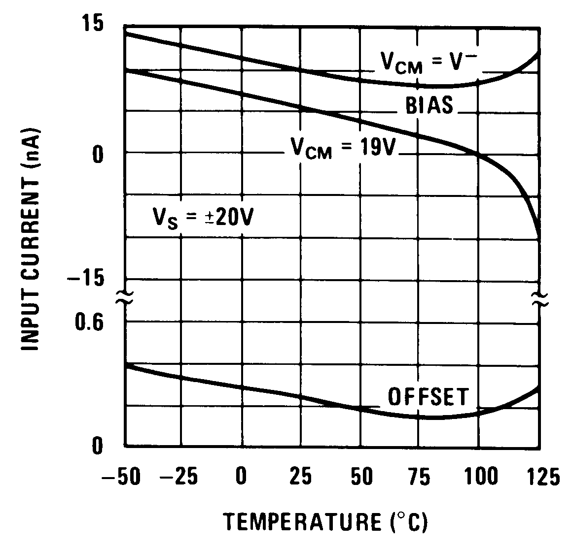
6.8.1 Typical Characteristics (Op Amp)









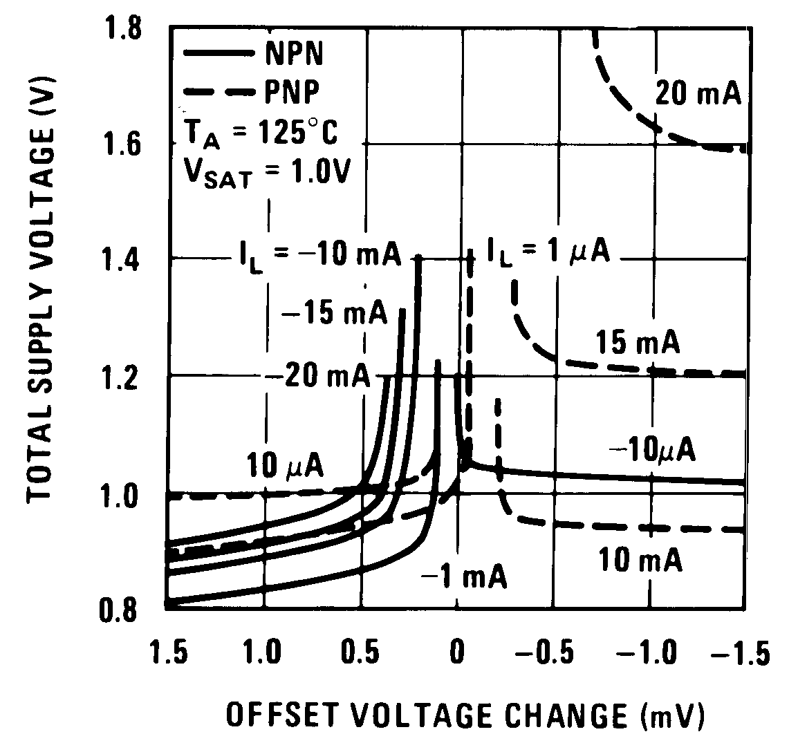

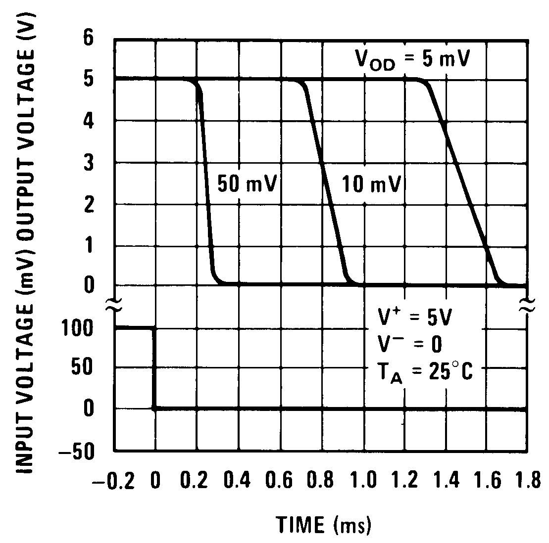

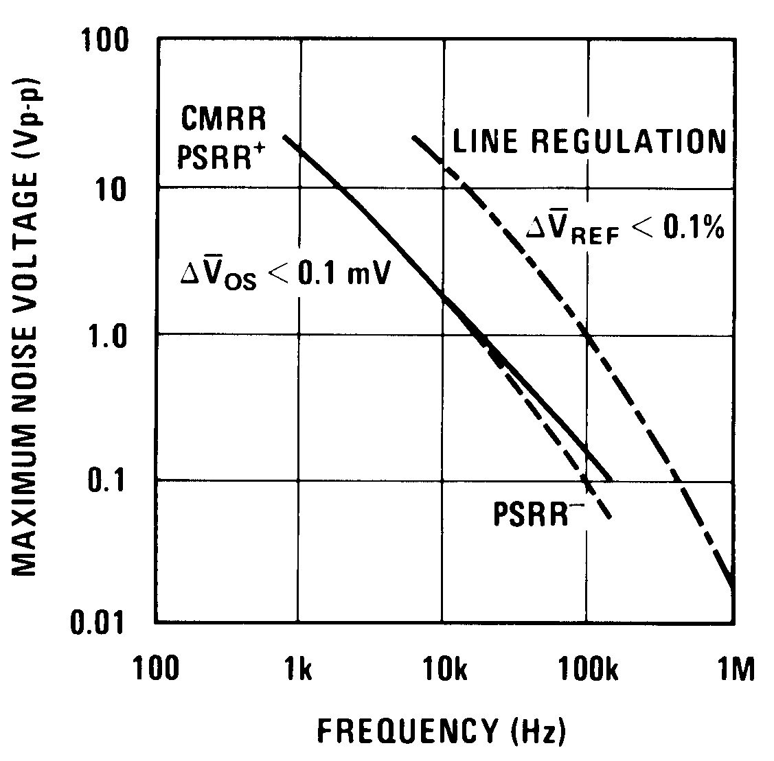


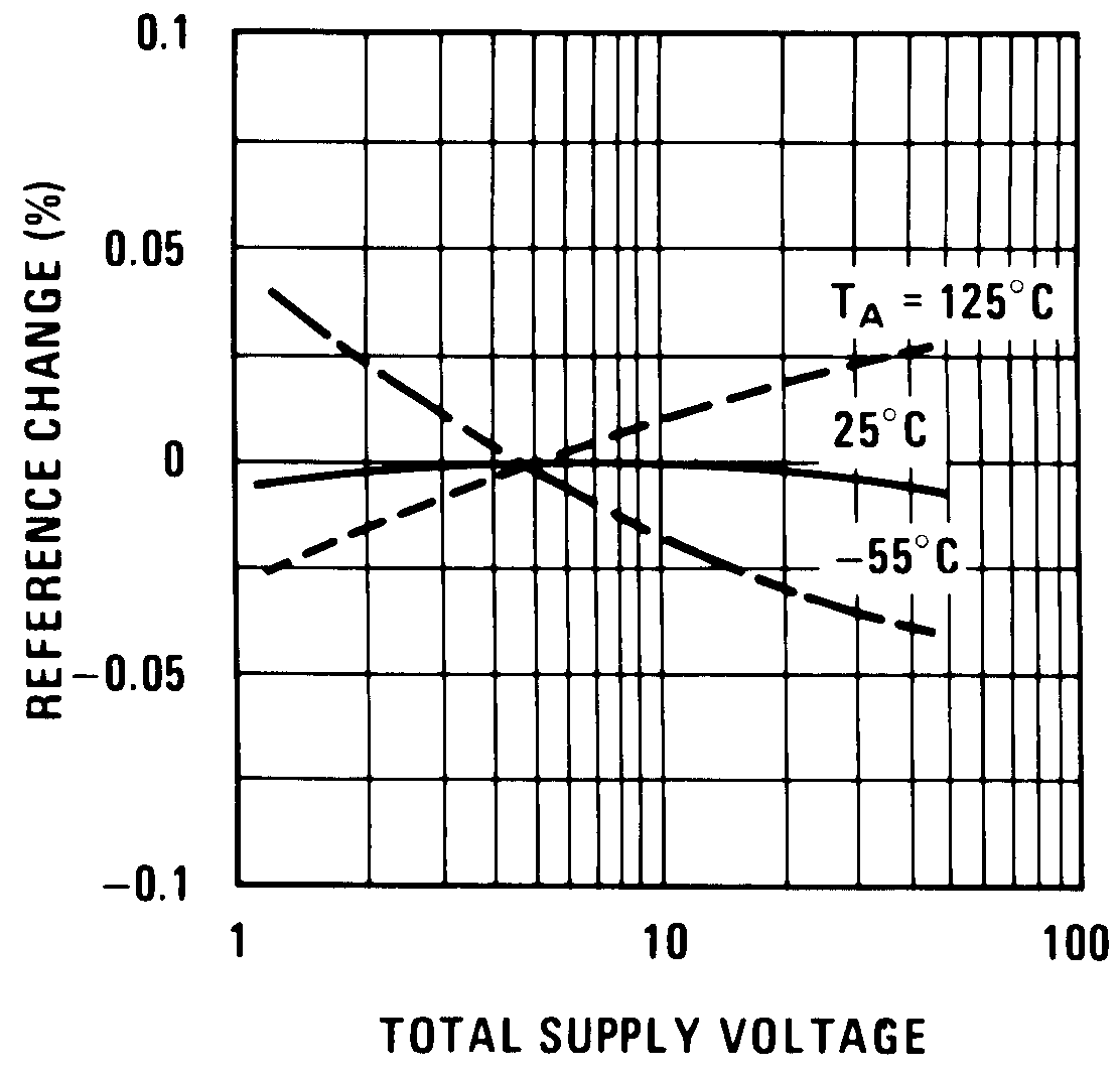
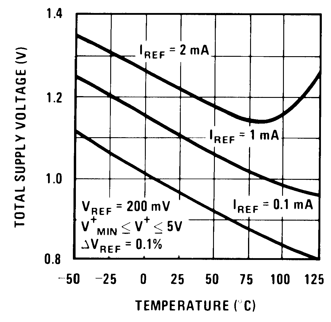
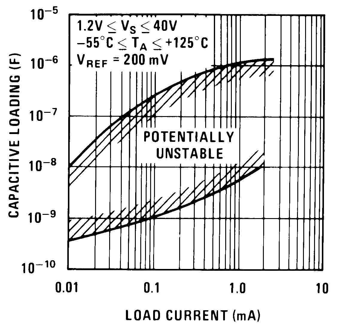
6.8.2 Typical Characteristics (Reference)
