SNVS729F September 2011 – August 2014 LM10506
PRODUCTION DATA.
- 1 Features
- 2 Applications
- 3 Description
- 4 Revision History
- 5 Device Comparison Table
- 6 Pin Configuration and Functions
-
7 Specifications
- 7.1 Absolute Maximum Ratings
- 7.2 Handling Ratings
- 7.3 Recommended Operating Conditions
- 7.4 Thermal Information
- 7.5 General Electrical Characteristics
- 7.6 Buck 1 Electrical Characteristics
- 7.7 Buck 2 Electrical Characteristics
- 7.8 Buck 3 Electrical Characteristics
- 7.9 LDO Electrical Characteristics
- 7.10 Comparators Electrical Characteristics
- 7.11 Typical Characteristics
-
8 Detailed Description
- 8.1 Functional Block Diagram
- 8.2 Feature Description
- 8.3 Device Functional Modes
- 8.4 Programming
-
9 Application and Implementation
- 9.1 Application Information
- 9.2 Typical Application
- 10Power Supply Recommendations
- 11Layout
- 12Device and Documentation Support
- 13Mechanical, Packaging, and Orderable Information
6 Pin Configuration and Functions
DSBGA
34
Top View
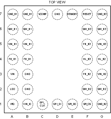
Pin Functions
| PIN | I/O(1) | TYPE(1) | DESCRIPTION | |
|---|---|---|---|---|
| NUMBER | NAME | |||
| A/B5 | VIN_B1 | I | P | Buck Switcher Regulator 1 - Power supply voltage input for power stage PFET. |
| A/B6 | SW_B1 | I/O | P | Buck Switcher Regulator 1 - Power Switching node, connect to inductor |
| A/B4 | FB_B1 | I/O | A | Buck Switcher Regulator 1 - Voltage output feedback plus Bypass Power |
| A/B7 | GND_B1 | G | P | Buck Switcher Regulator 1 - Power ground for Buck Regulator |
| G3 | VIN_B2 | I | P | Buck Switcher Regulator 2 - Power supply voltage input for power stage PFET. |
| F/G2 | SW_B2 | I/O | P | Buck Switcher Regulator 2 - Power Switching node, connect to inductor |
| F3 | FB_B2 | I | A | Buck Switcher Regulator 2 - Voltage output feedback |
| G1 | GND_B2 | G | P | Buck Switcher Regulator 2 - Power ground for Buck Regulator |
| G5 | VIN_B3 | I | P | Buck Switcher Regulator 3 - Power supply voltage input for power stage PFET. |
| F/G6 | SW_B3 | I/O | P | Buck Switcher Regulator 3 - Power Switching node, connect to inductor |
| F5 | FB_B3 | I | A | Buck Switcher Regulator 3 - Voltage output feedback |
| G7 | GND_B3 | G | P | Buck Switcher Regulator 3 - Power ground for Buck Regulator |
| A3 | VIN | I | P | Power supply Input Voltage, must be present for device to work |
| A2 | LDO | O | P | LDO Regulator - LDO regulator output voltage |
| G4 | HL_B2 | I | D | Digital Input Startup Control Signal to change predefined output Voltage of Buck 2, internally pulled down as a default |
| F4 | HL_B3 | I | D | Digital Input Startup Control Signal to change predefined output Voltage of Buck 3, internally pulled up as a default |
| E7 | STANDBY | I | D | Digital Input Control Signal for entering Standby Mode. This is an active High pin with an internal pulldown resistor. |
| F7 | RESET | I | D | Digital Input Control Signal to abort SPI transactions; resets the PMIC to default voltages. This is an active Low pin with an internal pullup. |
| C7 | VCOMP | I | A | Analog Input for Comparator |
| A1 | IRQ | O | D | Digital Output of Comparator to signal interrupt condition |
| F1 | SPI_CS | I | D | SPI Interface - chip select |
| D1 | SPI_DI | I | D | SPI Interface - serial data input |
| E1 | SPI_DO | O | D | SPI Interface - serial data output |
| C1 | SPI_CLK | I | D | SPI Interface - serial clock input |
| B1 | VIN_IO | I | A | Supply Voltage for Digital Interface |
| B2 | GND | G | G | Ground. Connect to system Ground. |
| B3 | GND | G | G | Ground. Connect to system Ground. |
| D7 | GND | G | G | Ground. Connect to system Ground. |
(1)
| Type | I/O | ||
| A | Analog Pin | I | Input Pin |
| D | Digital Pin | O | Output Pin |
| P | Power Connection | G | Ground |