SNVS729F September 2011 – August 2014 LM10506
PRODUCTION DATA.
- 1 Features
- 2 Applications
- 3 Description
- 4 Revision History
- 5 Device Comparison Table
- 6 Pin Configuration and Functions
-
7 Specifications
- 7.1 Absolute Maximum Ratings
- 7.2 Handling Ratings
- 7.3 Recommended Operating Conditions
- 7.4 Thermal Information
- 7.5 General Electrical Characteristics
- 7.6 Buck 1 Electrical Characteristics
- 7.7 Buck 2 Electrical Characteristics
- 7.8 Buck 3 Electrical Characteristics
- 7.9 LDO Electrical Characteristics
- 7.10 Comparators Electrical Characteristics
- 7.11 Typical Characteristics
-
8 Detailed Description
- 8.1 Functional Block Diagram
- 8.2 Feature Description
- 8.3 Device Functional Modes
- 8.4 Programming
-
9 Application and Implementation
- 9.1 Application Information
- 9.2 Typical Application
- 10Power Supply Recommendations
- 11Layout
- 12Device and Documentation Support
- 13Mechanical, Packaging, and Orderable Information
7 Specifications
7.1 Absolute Maximum Ratings
over operating free-air temperature range (unless otherwise noted) (1)(2)(3)| MIN | MAX | UNIT | ||
|---|---|---|---|---|
| VIN, VCOMP | −0.3 | 6 | V | |
| VIN_IO, VIN_B1, VIN_B2, VIN_B3, SPI_CS, SPI_DI, SPI_CLK, SPI_DO, IRQ, HL_B2, HL_B3, STANDBY, RESET, SW_B1, SW_B2, SW_B3, FB_B1, FB_B2, FB_B3, LDO | −0.3 | 6 | ||
| Junction Temperature (TJ-MAX) | 150 | °C | ||
(1) Stresses beyond those listed under Absolute Maximum Ratings may cause permanent damage to the device. These are stress ratings only, which do not imply functional operation of the device at these or any other conditions beyond those indicated under Recommended Operating Conditions. Exposure to absolute-maximum-rated conditions for extended periods may affect device reliability.
(2) Internal thermal shutdown protects device from permanent damage. Thermal shutdown engages at TJ = 140°C and disengages at TJ = 120°C (typ.). Thermal shutdown is ensured by design.
(3) If Military/Aerospace specified devices are required, please contact the Texas Instruments Sales Office/ Distributors for availability and specifications.
7.2 Handling Ratings
| MIN | MAX | UNIT | |||
|---|---|---|---|---|---|
| Tstg | Storage temperature range | –65 | 150 | °C | |
| V(ESD) | Electrostatic discharge | Human body model (HBM), per ANSI/ESDA/JEDEC JS-001, all pins(1) | –2000 | 2000 | V |
(1) JEDEC document JEP155 states that 500-V HBM allows safe manufacturing with a standard ESD control process.
7.3 Recommended Operating Conditions
over operating free-air temperature range (unless otherwise noted)| MIN | MAX | UNIT | ||
|---|---|---|---|---|
| VIN_B1, VIN_B2_VIN_B3, VIN | 3 | 5.5 | V | |
| VIN_IO (< VIN) | 1.72 | 3.63 (but < VIN) | ||
| All pins except VIN_IO | 0 | VIN | ||
| Junction temperature (TJ) | −40 | 125 | °C | |
| Ambient temperature (TA) | −40 | 85 | ||
| Maximum continuous power dissipation (PD-MAX) (1) | 0.9 | W | ||
(1) In applications where high power dissipation and/or poor thermal resistance is present the maximum ambient temperature may have to be derated. Maximum ambient temperature (TA-MAX) is dependent on the maximum operating junction temperature (TJ-MAX-OP = 125°C), the maximum power dissipation of the device in the application (PD-MAX), and the junction-to-ambient thermal resistance of the part/package in the application (RθJA), as given by the following equation: TA-MAX = TJ-MAX-OP – (RθJA × PD-MAX).
7.4 Thermal Information
| THERMAL METRIC(1) | LM10506 | UNIT | |
|---|---|---|---|
| DSBGA | |||
| 34 PINS | |||
| RθJA | Junction-to-ambient thermal resistance | 44.5 | °C/W |
(1) For more information about traditional and new thermal metrics, see the IC Package Thermal Metrics application report, SPRA953.
7.5 General Electrical Characteristics(2)(3)
Unless otherwise noted, VIN = 5 V where: VIN = VVIN_B1 = VVIN_B2 = VVIN_B3. Limits apply for TJ = 25°C, unless otherwise noted.| SYMBOL | PARAMETER | TEST CONDITIONS | MIN | TYP | MAX | UNIT |
|---|---|---|---|---|---|---|
| IQ(STANDBY) | Quiescent supply current | STANDBY = HIGH, no load | 100 | 200(4) | µA | |
| UNDER/OVERVOLTAGE LOCK OUT | ||||||
| VUVLO_RISING | 2.90 | V | ||||
| VUVLO_FALLING | 2.60 | |||||
| VOVLO_RISING | 5.82 | |||||
| VOVLO_FALLING | 5.70 | |||||
| DIGITAL INTERFACE | ||||||
| VIL | Logic input low | SPI_CS, SPI_DI, SPI_CLK, RESET, STANDBY | 0.3*VIN_IO(4) | V | ||
| VIH | Logic input high | 0.7*VIN_IO(4) | ||||
| VIL | Logic input low | HL_B2, HL_B3 | 0.3*VIN(4) | |||
| VIH | Logic input high | 0.7*VIN(4) | ||||
| VOL | Logic output low | SPI_DO, IRQ | 0.2*VIN_IO(4) | |||
| VOH | Logic output high | 0.8*VIN_IO(4) | ||||
| IIL | Input current, pin driven low | SPI_CS, SPI_DI, SPI_CLK, HL_B2, STANDBY | −2 | µA | ||
| HL_B3, RESET | −5 | |||||
| IIH | Input current, pin driven high | SPI_CS, SPI_DI, SPI_CLK, HL_B3, RESET | 2 | µA | ||
| HL_B2, STANDBY | 5 | |||||
| fSPI_MAX | SPI max frequency | 10(4) | MHz | |||
| tRESET | Minimum high-pulse width (1) | 2(4) | µs | |||
| tSTANDBY | 2(4) | |||||
(1) Specification ensured by design. Not tested during production.
(2) All limits are ensured by design, test and/or statistical analysis. All electrical characteristics having room-temperature limits are tested during production with TJ = 25°C. All hot and cold limits are ensured by correlating the electrical characteristics to process and temperature variations and applying statistical process control.
(3) Capacitors: Low-ESR Surface-Mount Ceramic Capacitors (MLCCs) are used in setting electrical characteristics.
(4) Limits apply over the entire operating junction temperature range of −40°C ≤ TA = TJ ≤ 85°C.
7.6 Buck 1 Electrical Characteristics(2)(3)(4)
Unless otherwise noted, VIN = 5 V where: VIN = VVIN_B1 = VVIN_B2 = VVIN_B3. Limits apply for TJ = 25°C, unless otherwise noted.| SYMBOL | PARAMETER | TEST CONDITIONS | MIN | TYP | MAX | UNIT |
|---|---|---|---|---|---|---|
| IQ | DC bias current in VIN | No Load, PFM Mode | 15 | 50(5) | µA | |
| IPEAK | Peak switching current limit | Buck 1 enabled, switching in PWM | 1.6(5) | 1.8 | 2.1(5) | A |
| η | Efficiency peak, Buck 1 (1) | IOUT = 0.3 A | 90% | |||
| ƒSW | Switching frequency | 1.75(5) | 2 | 2.3(5) | MHz | |
| CIN | Input capacitor (1) | 0 mA ≤ IOUT ≤ 1.3 A | 4.7 | µF | ||
| COUT | Output filter capacitor (1) | 10 | 10 | 100 | ||
| Output capacitor ESR (1) | 20 | mΩ | ||||
| L | Output filter inductance (1) | 2.2 | µH | |||
| ΔVOUT | DC line regulation (1) | 3.3 V ≤ VIN ≤ 5 V, IOUT = 1.3 A | 0.5 | %/V | ||
| DC load regulation (1) | 0.13 A ≤ IOUT ≤ 1.3 A | 0.3 | %/A | |||
| IFB | Feedback pin input bias current | VFB = 3 V | 2.1 | 5(5) | µA | |
| RDS-ON-HS | High side switch on resistance | 135 | mΩ | |||
| VIN = 2.6 V | 215 | |||||
| RDS-ON-LS | Low side switch on resistance | 85 | 190(5) | mΩ | ||
| RDS-ON_BYPASS | Bypass FET on resistance | Used in parallel with the high side FET while in Bypass mode. Resistance (DCR) of inductor = 100 mΩ | ||||
| VIN = 3.3 V | 85 | mΩ | ||||
| VIN = 2.6 V | 120 | |||||
| STARTUP | ||||||
| TSTART | Internal soft-start (turn on time) (1) | Start-up from shutdown, VOUT = 0V, no load, LC = recommended circuit, using software enable, to VOUT = 95% of final value | 0.1 | ms | ||
(1) Specification ensured by design. Not tested during production.
(2) All limits are ensured by design, test and/or statistical analysis. All electrical characteristics having room-temperature limits are tested during production with TJ = 25°C. All hot and cold limits are ensured by correlating the electrical characteristics to process and temperature variations and applying statistical process control.
(3) Capacitors: Low-ESR Surface-Mount Ceramic Capacitors (MLCCs) are used in setting electrical characteristics.
(4) BUCK normal operation is ensured if VIN ≥ VOUT+1 V.
(5) Limits apply over the entire operating junction temperature range of −40°C ≤ TA = TJ ≤ 85°C.
7.7 Buck 2 Electrical Characteristics(2)(3)(4)
Unless otherwise noted, VIN = 5 V where: VIN = VVIN_B1 = VVIN_B2 = VVIN_B3. Limits apply for TJ = 25°C, unless otherwise noted.| SYMBOL | PARAMETER | TEST CONDITIONS | MIN | TYP | MAX | UNIT |
|---|---|---|---|---|---|---|
| IQ | DC bias current in VIN | No Load, PFM Mode | 15 | 50(5) | µA | |
| IPEAK | Peak switching current limit | Buck 2 enabled, switching in PWM | 0.65(5) | 1.1 | 1.55(5) | A |
| η | Efficiency peak, Buck 2 (1) | IOUT = 0.3 A | 90% | |||
| ƒSW | Switching frequency | 1.75(5) | 2 | 2.3(5) | MHz | |
| CIN | Input capacitor (1) | 0 mA ≤ IOUT ≤ 400 mA | 4.7 | µF | ||
| COUT | Output filter capacitor (1) |
10 | 10 | 100 | ||
| Output capacitor ESR (1) | 20 | mΩ | ||||
| L | Output filter inductance (1) | 2.2 | µH | |||
| ΔVOUT | DC line regulation (1) | 3.3 V ≤ VIN ≤ 5 V, IOUT = 400 mA | 0.5 | %/V | ||
| DC load regulation (1) | 100 mA ≤ IOUT ≤ 400 mA | 0.3 | %/A | |||
| IFB | Feedback pin input bias current | VFB = 1.8 V | 1.8 | 5(5) | µA | |
| RDS-ON-HS | High side switch on resistance | 135 | mΩ | |||
| VIN = 2.6 V | 260 | |||||
| RDS-ON-LS | Low side switch on resistance | 85 | 190(5) | |||
| STARTUP | ||||||
| TSTART | Internal soft-start (turn on time) (1) | Startup from shutdown, VOUT = 0V, no load, LC = recommended circuit, using software enable, to VOUT = 95% of final value | 0.1 | ms | ||
(1) Specification ensured by design. Not tested during production.
(2) All limits are ensured by design, test and/or statistical analysis. All electrical characteristics having room-temperature limits are tested during production with TJ = 25°C. All hot and cold limits are ensured by correlating the electrical characteristics to process and temperature variations and applying statistical process control.
(3) Capacitors: Low-ESR Surface-Mount Ceramic Capacitors (MLCCs) are used in setting electrical characteristics.
(4) BUCK normal operation is ensured if VIN ≥ VOUT+1 V.
(5) Limits apply over the entire operating junction temperature range of −40°C ≤ TA = TJ ≤ 85°C.
7.8 Buck 3 Electrical Characteristics(2)(3)(4)
Unless otherwise noted, VIN = 5 V where: VIN = VVIN_B1 = VVIN_B2 = VVIN_B3. Limits apply for TJ = 25°C, unless otherwise noted.| SYMBOL | PARAMETER | TEST CONDITIONS | MIN | TYP | MAX | UNIT |
|---|---|---|---|---|---|---|
| IQ | DC bias current in VIN | No Load, PFM Mode | 15 | 50(5) | µA | |
| IPEAK | Peak switching current limit | Buck 3 enabled, switching in PWM | 0.9(5) | 1.2 | 1.7(5) | A |
| η | Efficiency peak, Buck 3 (1) | IOUT = 0.3 A | 90% | |||
| ƒSW | Switching frequency | 1.75(5) | 2 | 2.3(5) | MHz | |
| CIN | Input Capacitor (1) | 0 mA ≤ IOUT ≤ 600 mA | 4.7 | µF | ||
| COUT | Output Filter Capacitor (1) | 10 | 10 | 100 | ||
| Output Capacitor ESR (1) | 20 | mΩ | ||||
| L | Output Filter Inductance (1) | 2.2 | µH | |||
| ΔVOUT | DC Line regulation (1) | 3.3 V ≤ VIN ≤ 5 V, IOUT = 600 mA | 0.5 | %/V | ||
| DC Load regulation (1) | 150 mA ≤ IOUT ≤ 600 mA | 0.3 | %/A | |||
| IFB | Feedback pin input bias current | VFB = 1.2 V | 0.9 | 5(5) | µA | |
| RDS-ON-HS | High Side Switch On Resistance | 135 | mΩ | |||
| VIN = 2.6 V | 260 | |||||
| RDS-ON-LS | Low Side Switch On Resistance | 85 | 190(5) | |||
| STARTUP | ||||||
| TSTART | Internal soft-start (turn on time) (1) | Startup from shutdown, VOUT = 0 V, no load, LC = recommended circuit, using software enable, to VOUT = 95% of final value | 0.1 | ms | ||
(1) Specification ensured by design. Not tested during production.
(2) All limits are ensured by design, test and/or statistical analysis. All electrical characteristics having room-temperature limits are tested during production with TJ = 25°C. All hot and cold limits are ensured by correlating the electrical characteristics to process and temperature variations and applying statistical process control.
(3) Capacitors: Low-ESR Surface-Mount Ceramic Capacitors (MLCCs) are used in setting electrical characteristics.
(4) BUCK normal operation is ensured if VIN ≥ VOUT+1 V.
(5) Limits apply over the entire operating junction temperature range of −40°C ≤ TA = TJ ≤ 85°C.
7.9 LDO Electrical Characteristics(2)(3)
Unless otherwise noted, VIN = 5 V where: VIN = VVIN_B1 = VVIN_B2 = VVIN_B3. Limits apply for TJ = 25°C, unless otherwise noted.| PARAMETER | TEST CONDITIONS | MIN | TYP | MAX | UNIT | ||
|---|---|---|---|---|---|---|---|
| VOUT | Output voltage accurancy | IOUT = 1 mA | –3%(4) | 3%(4) | |||
| ISC | Short-circuit current limit | VOUT = 0 V | 0.3 | ||||
| VIN = 3.3 V, VOUT = 0 V (1) | 0.5 | ||||||
| VDO | Dropout voltage | IOUT = 100 mA | 60 | 100(4) | mV | ||
| ΔVOUT | Line regulation | 3.3 V ≤ VIN ≤ 5.5 V, IOUT = 1 mA | 5 | ||||
| Load regulation | 1 mA ≤ IOUT ≤ 100 mA, VIN = 3.3 V, 5 V | 5 | |||||
| eN | Output noise voltage(1) | 10 Hz ≤ ƒ ≤ 100 kHz | VIN = 5 V | 10 | µVRMS | ||
| VIN = 3.3 V | 35 | ||||||
| PSSR | Power supply rejection ratio(1) | F = 10 kHz, COUT = 4.7 µF, IOUT = 20 mA |
VIN = 5 V | 65 | dB | ||
| VIN = 3.3 V | 40 | ||||||
| tSTARTUP | Start-up time from shutdown(1) | COUT = 4.7 µF, IOUT = 100 mA | VIN = 5 V | 45 | µs | ||
| VIN = 3.3 V | 60 | ||||||
| tTRANSIENT | Start-up transient overshoot(1) | 30(4) | mV | ||||
(1) Specification ensured by design. Not tested during production.
(2) All limits are ensured by design, test and/or statistical analysis. All electrical characteristics having room-temperature limits are tested during production with TJ = 25°C. All hot and cold limits are ensured by correlating the electrical characteristics to process and temperature variations and applying statistical process control.
(3) Capacitors: Low-ESR Surface-Mount Ceramic Capacitors (MLCCs) are used in setting electrical characteristics.
(4) Limits apply over the entire operating junction temperature range of −40°C ≤ TA = TJ ≤ 85°C.
7.10 Comparators Electrical Characteristics(1)(2)
Unless otherwise noted, VIN = 5 V where: VIN = VIN_B1 = VIN_B2 = VIN_B3. Limits apply for TJ = 25°C, unless otherwise noted.| SYMBOL | PARAMETER | TEST CONDITIONS | MIN | TYP | MAX | UNIT |
|---|---|---|---|---|---|---|
| IVCOMP | VCOMP pin bias current | VCOMP = 0 V | 0.1 | 2(3) | µA | |
| VCOMP = 5 V | 0.1 | 2(3) | ||||
| VCOMP_RISE | Comparator rising edge trigger level | 2.826 | V | |||
| VCOMP_FALL | Comparator falling edge trigger level | 2.768 | ||||
| Hysteresis | 30(3) | 60 | 80(3) | mV | ||
| IRQVOH | Output voltage high | 0.8*VIN_IO(3) | V | |||
| IRQVOL | Output voltage low | 0.2*VIN_IO(3) | ||||
| tCOMP | Transition time of IRQ output | 6 | 15(3) | µsec |
(1) All limits are ensured by design, test and/or statistical analysis. All electrical characteristics having room-temperature limits are tested during production with TJ = 25°C. All hot and cold limits are ensured by correlating the electrical characteristics to process and temperature variations and applying statistical process control.
(2) Capacitors: Low-ESR Surface-Mount Ceramic Capacitors (MLCCs) are used in setting electrical characteristics.
(3) Limits apply over the entire operating junction temperature range of −40°C ≤ TA = TJ ≤ 85°C.
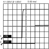
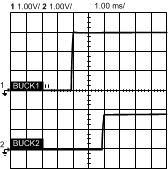
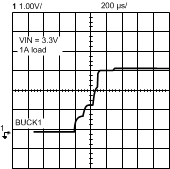
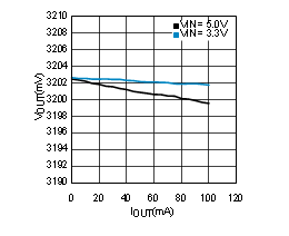
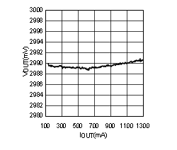
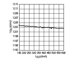
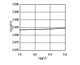
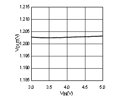
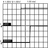
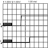
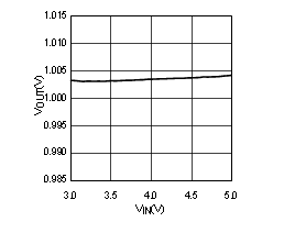
7.11 Typical Characteristics
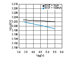
| VIN = 3.3 V | VOUT = 3 V | IOUT = 1 A |
| VIN = 5 V | VOUT = 3 V | |
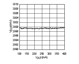
| VIN = 5 V | VOUT = 3 V | |
| VIN = 5 V | VOUT = 1.2 V | |
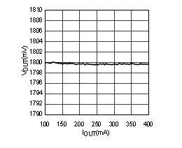
| VOUT = 3 V | IOUT = 400 mA | |
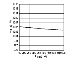
| VOUT = 1.2 V | IOUT = 600 mA | |
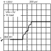
| VIN = 5 V | VOUT = 3 V | IOUT = 1 A |
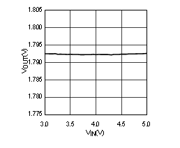
| VIN = 5 V | VOUT = 1.8 V | |
| VIN = 5 V | VOUT = 1 V | |
| VOUT = 1.8 V | IOUT = 400 mA | |
| VOUT = 1 V | IOUT = 600 mA | |