SNVS999 May 2014 LM10507
PRODUCTION DATA.
- 1 Features
- 2 Applications
- 3 Description
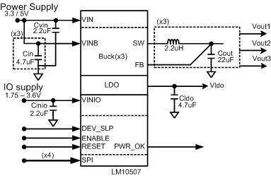
- 4 Simplified Schematic
- 5 Revision History
- 6 Pin Configuration and Functions
-
7 Specifications
- 7.1 Absolute Maximum Ratings
- 7.2 Handling Ratings
- 7.3 Recommended Operating Conditions
- 7.4 Thermal Information
- 7.5 General Electrical Characteristics
- 7.6 Buck 1 Electrical Characteristics
- 7.7 Buck 2 Electrical Characteristics
- 7.8 Buck 3 Electrical Characteristics
- 7.9 LDO Electrical Characteristics
- 7.10 Typical Characteristics
-
8 Detailed Description
- 8.1 Overview
- 8.2 Functional Block Diagram
- 8.3 Feature Description
- 8.4
Device Functional Modes
- 8.4.1 PWM Operation
- 8.4.2 PFM Operation (Bucks 1, 2 & 3)
- 8.4.3 Soft Start
- 8.4.4 Current Limiting
- 8.4.5 Internal Synchronous Rectification
- 8.4.6 Low Dropout Operation
- 8.4.7
Device Operating Modes
- 8.4.7.1 Startup Sequence
- 8.4.7.2 Power-On Default and Device Enable
- 8.4.7.3 RESET: Pin Function
- 8.4.7.4 DEVSLP (Device Sleep) Function
- 8.4.7.5 DEVSLP Terminal
- 8.4.7.6 Device Sleep (DEVSLP) Programming via SPI
- 8.4.7.7 ENABLE, Function
- 8.4.7.8 Under Voltage Lock Out (UVLO)
- 8.4.7.9 Over Voltage Lock Out (OVLO)
- 8.4.7.10 PWR_OK - Pin Function
- 8.4.7.11 Thermal Shutdown (TSD)
- 8.5 Programming
- 8.6 Register Maps
-
9 Applications and Implementation
- 9.1 Application Information
- 9.2
Typical Application
- 9.2.1 Design Requirements
- 9.2.2
Detailed Design Procedure
- 9.2.2.1 Input Voltage
- 9.2.2.2 Output Enable
- 9.2.2.3 Recommendations for Unused Functions and Pins
- 9.2.2.4 External Components Selection
- 9.2.2.5 Output Inductors and Capacitors Selection
- 9.2.2.6 Inductor Selection
- 9.2.2.7 Recommended Method for Inductor Selection
- 9.2.2.8 Alternate Method for Inductor Selection
- 9.2.2.9 Suggested Inductors and Their Suppliers
- 9.2.2.10 Output and Input Capacitors Characteristics
- 9.2.2.11 Output Capacitor Selection
- 9.2.2.12 Input Capacitor Selection
- 9.2.3 Application Performance Plots
- 10Power Supply Recommendations
- 11Layout
- 12Device and Documentation Support
- 13Mechanical, Packaging, and Orderable Information
1 Features
- Three Highly Efficient Programmable Buck Regulators
- Integrated FETs with Low RDS-ON
- Bucks Operate with their Phases Shifted to Reduce the Input Current Ripple and Capacitor Size
- Programmable Output Voltage via the SPI Interface
- Over and Under-Voltage-Lockout
- Automatic Internal Soft Start with Power-On Reset
- Current Overload and Thermal Shutdown Protection
- PFM Mode for High Efficiency at Light Load Conditions
- Low-Dropout Regulator 2.5 V, 250mA
- Hardware ENABLE and PWR_OK Terminal
- Fast Start-up for All Voltage Rails in about 3.5ms to PWR_OK
- Fast Turn-off / Active Discharge on Regulator Outputs
- Programmable Buck Regulators:
- Buck 1: 0.9 - 3.4 V; 1.6A
- Buck 2: 0.9 - 3.4 V; 1A
- Buck 3: 0.865 - 1.5 V; 1A
- ±3% Feedback Voltage Accuracy
- Up to 95% efficient Buck Regulators
- 2MHz Switching Frequency for Smaller Inductor Size
- 2.8 x 2.8 mm, 0.4 mm pitch, 34-bump µSMD Package
2 Applications
Solid-State Drives
3 Description
The LM10507 is an advanced PMU containing three configurable, high-efficiency buck regulators for supplying variable voltages. The device is ideal for supporting ASIC and SOC designs for Solid-State and Flash drives.
LM10507 operates cooperatively with ASIC to optimize the supply voltage for low power conditions and power saving modes via SPI interface. It also supports a 2.5 V 250 mA LDO.
Device Information(1)
| PART NUMBER | PACKAGE | BODY SIZE (NOM) |
|---|---|---|
| LM10507 | DSBGA (34) | 2.82 mm x 2.82 mm |
- For all available packages, see the orderable addendum at the end of the datasheet.
4 Simplified Schematic