SNVS999 May 2014 LM10507
PRODUCTION DATA.
- 1 Features
- 2 Applications
- 3 Description
- 4 Simplified Schematic
- 5 Revision History
- 6 Pin Configuration and Functions
-
7 Specifications
- 7.1 Absolute Maximum Ratings
- 7.2 Handling Ratings
- 7.3 Recommended Operating Conditions
- 7.4 Thermal Information
- 7.5 General Electrical Characteristics
- 7.6 Buck 1 Electrical Characteristics
- 7.7 Buck 2 Electrical Characteristics
- 7.8 Buck 3 Electrical Characteristics
- 7.9 LDO Electrical Characteristics
- 7.10 Typical Characteristics
-
8 Detailed Description
- 8.1 Overview
- 8.2 Functional Block Diagram
- 8.3 Feature Description
- 8.4
Device Functional Modes
- 8.4.1 PWM Operation
- 8.4.2 PFM Operation (Bucks 1, 2 & 3)
- 8.4.3 Soft Start
- 8.4.4 Current Limiting
- 8.4.5 Internal Synchronous Rectification
- 8.4.6 Low Dropout Operation
- 8.4.7
Device Operating Modes
- 8.4.7.1 Startup Sequence
- 8.4.7.2 Power-On Default and Device Enable
- 8.4.7.3 RESET: Pin Function
- 8.4.7.4 DEVSLP (Device Sleep) Function
- 8.4.7.5 DEVSLP Terminal
- 8.4.7.6 Device Sleep (DEVSLP) Programming via SPI
- 8.4.7.7 ENABLE, Function
- 8.4.7.8 Under Voltage Lock Out (UVLO)
- 8.4.7.9 Over Voltage Lock Out (OVLO)
- 8.4.7.10 PWR_OK - Pin Function
- 8.4.7.11 Thermal Shutdown (TSD)
- 8.5 Programming
- 8.6 Register Maps
-
9 Applications and Implementation
- 9.1 Application Information
- 9.2
Typical Application
- 9.2.1 Design Requirements
- 9.2.2
Detailed Design Procedure
- 9.2.2.1 Input Voltage
- 9.2.2.2 Output Enable
- 9.2.2.3 Recommendations for Unused Functions and Pins
- 9.2.2.4 External Components Selection
- 9.2.2.5 Output Inductors and Capacitors Selection
- 9.2.2.6 Inductor Selection
- 9.2.2.7 Recommended Method for Inductor Selection
- 9.2.2.8 Alternate Method for Inductor Selection
- 9.2.2.9 Suggested Inductors and Their Suppliers
- 9.2.2.10 Output and Input Capacitors Characteristics
- 9.2.2.11 Output Capacitor Selection
- 9.2.2.12 Input Capacitor Selection
- 9.2.3 Application Performance Plots
- 10Power Supply Recommendations
- 11Layout
- 12Device and Documentation Support
- 13Mechanical, Packaging, and Orderable Information
9 Applications and Implementation
9.1 Application Information
The LM10507 device provides 4 regulated outputs from 3 step-down switching regulators and one linear regulator. The regulated outputs are achieved using a minimum of external components. The device outputs are controlled via an ENABLE input with control for a sleep mode via a further input, DEV_SLP.
A 4-wire SPI interface may be used to reconfigure the device outputs and return an indication of output status. A separate device output also provides a digital indication of output status. All programmed settings may be returned to default state via a RESET input.
9.2 Typical Application
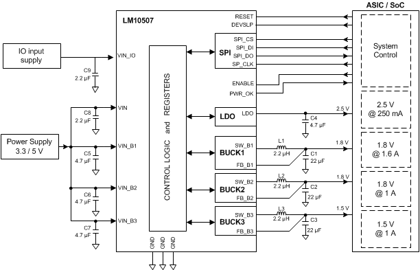 Figure 11. Typical Application Diagram
9.2.1 Design Requirements
| Regulator | Default VOUT DEVSLP=Low | Default VOUT DEVSLP=High | VOUT Range | Maximum Output Current |
|---|---|---|---|---|
| BUCK 1 | 1 V | OFF | 0.9 – 3.4 V; 50mV steps | 1.6 A |
| BUCK 2 | 1.8 V | OFF | 0.9 – 3.4 V; 50mV steps | 1 A |
| BUCK 3 | 1.5 V | 1.5 V | 0.865-1.5 V; 5mV steps | 1 A |
| LDO | 2.5 V | OFF | 2.5 V | 250 mA |
Default voltage values are determined when working in PWM mode. Voltage may be 0.8-1.6% higher when in PFM mode.
9.2.2 Detailed Design Procedure
9.2.2.1 Input Voltage
VIN, VIN_B1, VIN_B2 and VIN_B3 must all be connected to the same power source.
9.2.2.2 Output Enable
For normal operation it is recommended that the ENABLE input is controlled via an independent voltage applied to the input.
To enable the device outputs at device power up the ENABLE input may be connected to the supply voltage either directly or via a divider to the input supply to ensure correct voltage within the specified range. In this case start up timing may vary from the specified values depending on the supply start up slew rate.
9.2.2.3 Recommendations for Unused Functions and Pins
If any function is not used in the end application then the following recommendations for tying-off the associated pins on the circuit boards should be used.
| FUNCTION | PIN | IF UNUSED |
|---|---|---|
| BUCK1 | VIN_B1 | Connect to VIN |
| SW_B1 | Connect to VIN | |
| FB_B1 | Connect to GND | |
| BUCK2 | VIN_B2 | Connect to VIN |
| SW_B2 | Connect to VIN | |
| FB_B2 | Connect to GND | |
| BUCK3 | VIN_B3 | Connect to VIN |
| SW_B3 | Connect to VIN | |
| FB_B3 | Connect to GND | |
| SPI | SPI_CS | Connect to VIN_IO |
| SPI_DI | Connect to GND | |
| SPI_DO | Connect to GND | |
| SPI_CK | Connect to GND | |
| DEVSLP | Connect to GND | |
| CONTROL and MONITOR | RESET | Connect to VIN_IO |
| PWR_OK | Leave open |
9.2.2.4 External Components Selection
All three switchers require an input capacitor, and an output inductor-capacitor filter. These components are critical to the performance of the device. All three switchers are internally compensated and do not require external components to achieve stable operation. The output voltage of the Bucks can be programmed through the SPI terminals.
9.2.2.5 Output Inductors and Capacitors Selection
There are several design considerations related to the selection of output inductors and capacitors:
- Load transient response
- Stability
- Efficiency
- Output ripple voltage
- Over current ruggedness
The device has been optimized for use with nominal LC values as shown in the Application Diagram.
9.2.2.6 Inductor Selection
The recommended inductor values are shown in the Application Diagram. It is important to guarantee the inductor core does not saturate during any foreseeable operational situation. The inductor should be rated to handle the peak load current plus the ripple current: Care should be taken when reviewing the different saturation current ratings that are specified by different manufacturers. Saturation current ratings are typically specified at 25C, so ratings at maximum ambient temperature of the application should be requested from the manufacturer.
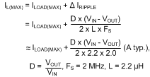
where
- IL(MAX) : Max inductor Current
- ILOAD(MAX): Max load current
- IRIPPLE : Peak-to-Peak inductor current
- D : Estimated duty factor
- VIN : Input voltage
- VOUT : Output voltage
- FS : Switching frequency, Hertz
There are two methods to choose the inductor saturation current rating:
9.2.2.7 Recommended Method for Inductor Selection
The best way to guarantee the inductor does not saturate is to choose an inductor that has saturation current rating greater than the maximum device current limit, as specified in the Electrical Characteristics. In this case the device will prevent inductor saturation by going into current limit before the saturation level is reached.
9.2.2.8 Alternate Method for Inductor Selection
If the recommended approach cannot be used care must be taken to guarantee that the saturation current is greater than the peak inductor current:
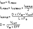
where
- ISAT : Inductor saturation current at operating temperature
- ILPEAK : Peak inductor current during worst case conditions
- IOUTMAX : Maximum average inductor current
- IRIPPLE : Peak-to-Peak inductor current
- VOUT : Output voltage
- VIN : Input voltage (VVIN_B1, VVIN_B2, VVIN_B3)
- L : Inductor value in Henries at IOUTMAX
- FS : Switching frequency, Hertz
- D : Estimated duty factor
- EFF : Estimated power supply efficiency
ISAT may not be exceeded during any operation, including transients, startup, high temperature, worst case conditions, etc.
9.2.2.9 Suggested Inductors and Their Suppliers
The designer should choose the inductors that best match the system requirements. A very wide range of inductors are available as regarding physical size, height, maximum current (thermally limited, and inductance loss limited), series resistance, maximum operating frequency, losses, etc. In general, smaller physical size inductors will have higher series resistance (DCR) and implicitly lower overall efficiency is achieved. Very low profile inductors may have even higher series resistance. The designer should try to find the best compromise between system performance and cost.
Table 1. Typical Recommended Inductors
| Value | Mfr | Part Number | DCR | Current | Package |
|---|---|---|---|---|---|
| 2.2µH | Murata | LQH55PN2R2NR0L | 31mOhms | 2.5A | 2220 |
| 2.2µH | TDK | NLC565050T-2R2K-PF | 60mOhms | 1.3A | 2220 |
| 2.2µH | Murata | LQM2MPN2R2NG0 | 110mOhms | 1.2A | 806 |
| 2.2uH | Vishay Dale | IFSC1008ABER2R2M01 | 80mOhms | 1.85A | 2.5 x 2.0 |
| 2.2uH | Taiyo Yuden | MAMK2520T2R2M | 117mOhm | 1.9A | 2.5 x 2.0 |
9.2.2.10 Output and Input Capacitors Characteristics
Special attention should be paid when selecting these components. As shown in the following figure, the DC bias of these capacitors can result in a capacitance value that falls below the minimum value given in the recommended capacitor specifications table. Note that the graph shows the capacitance out of spec for the 0402 case size capacitor at higher bias voltages. It is therefore recommended that the capacitor manufacturers’ specifications for the nominal value capacitor are consulted for all conditions, as some capacitor sizes (e.g. 0402) may not be suitable in the actual application.
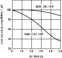 Figure 12. Typical Variation in Capacitance vs. DC Bias
The ceramic capacitor’s actual capacitance can vary with temperature. The capacitor type X7R, which operates over a temperature range of −55°C to +125°C, will only vary the capacitance to within ±15%. The capacitor type X5R has a similar tolerance over a reduced temperature range of −55°C to +85°C. Many large value ceramic capacitors, larger than 1 μF are manufactured with Z5U or Y5V temperature characteristics. Their capacitance can drop by more than 50% as the temperature varies from 25°C to 85°C. Therefore X5R or X7R is recommended over Z5U and Y5V in applications where the ambient temperature will change significantly above or below 25°C.
Tantalum capacitors are less desirable than ceramic for use as output capacitors because they are more expensive when comparing equivalent capacitance and voltage ratings in the 0.47 μF to 44 μF range. Another important consideration is that tantalum capacitors have higher ESR values than equivalent size ceramics. This means that while it may be possible to find a tantalum capacitor with an ESR value within the stable range, it would have to be larger in capacitance (which means bigger and more costly) than a ceramic capacitor with the same ESR value. It should also be noted that the ESR of a typical tantalum will increase about 2:1 as the temperature goes from 25°C down to −40°C, so some guard band must be allowed.
9.2.2.11 Output Capacitor Selection
The output capacitor of a switching converter absorbs the AC ripple current from the inductor and provides the initial response to a load transient. The ripple voltage at the output of the converter is the product of the ripple current flowing through the output capacitor and the impedance of the capacitor. The impedance of the capacitor can be dominated by capacitive, resistive, or inductive elements within the capacitor, depending on the frequency of the ripple current. Ceramic capacitors have very low ESR and remain capacitive up to high frequencies. Their inductive component can be usually neglected at the frequency ranges the switcher operates.
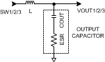 Figure 13. Output Filter
The output-filter capacitor smoothes out the current flow from the inductor to the load and helps maintain a steady output voltage during transient load changes. It also reduces output voltage ripple. These capacitors must be selected with sufficient capacitance and low enough ESR to perform these functions. Note that the output voltage ripple increases with the inductor current ripple and the Equivalent Series Resistance of the output capacitor (ESRCOUT). Also note that the actual value of the capacitor’s ESRCOUT is frequency and temperature dependent, as specified by its manufacturer. The ESR should be calculated at the applicable switching frequency and ambient temperature.

where
- VOUT-RIPPLE-PP : estimated output voltage ripple
- IRIPPLE : estimated current ripple
- D : Estimated duty factor
Output ripple can be estimated from the vector sum of the reactive (capacitance) voltage component and the real (ESR) voltage component of the output capacitor:


where
- VOUT-RIPPLE-PP : estimated output ripple,
- VROUT : estimated real output ripple,
- VCOUT : estimated reactive output ripple.
The device is designed to be used with ceramic capacitors on the outputs of the buck regulators. The recommended dielectric type of these capacitors is X5R, X7R, or of comparable material to maintain proper tolerances over voltage and temperature. The recommended value for the output capacitors is 22 μF, 6.3V with an ESR of 2mΩ or less. The output capacitors need to be mounted as close as possible to the output/ground terminals of the device.
Table 2. Typical Recommended Output Capacitors
| Model | Vendor Type | Vendor | Voltage Rating | Inch (mm) Case Size |
|---|---|---|---|---|
| 08056D226MAT2A | Ceramic, X5R | AVX Corporation | 6.3 V | 0805, (2012) |
| C0805L226M9PACTU | Ceramic, X5R | Kemet | 6.3 V | 0805, (2012) |
| ECJ-2FB0J226M | Ceramic, X5R | Panasonic – ECG | 6.3 V | 0805, (2012) |
| JMK212BJ226MG-T | Ceramic, X5R | Taiyo Yuden | 6.3 V | 0805, (2012) |
| C2012X5R0J226M | Ceramic, X5R | TDK Corporation | 6.3 V | 0805, (2012) |
| GRM188R60G226MEA0L | Ceramic, X5R | Murata | 4.0 V | 0603 |
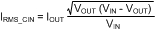
9.2.2.12 Input Capacitor Selection
There are 3 buck regulators in the LM10507 device. Each of these buck regulators has its own input capacitor which should be located as close as possible to their corresponding VIN_Bx and GND_Bx terminals, where x designates the buck 1,2 or 3. The 3 buck regulators operate at 120o out of phase, which means that is they switch on at equally spaced intervals, in order to reduce the input power rail ripple. It is recommended to connect all the supply/ground terminals of the buck regulators, VIN_Bx to two solid internal planes located under the device. In this way, the 3 input capacitors work together and further reduce the input current ripple. A larger tantalum capacitor can also be located in the proximity of the device.
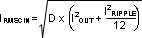
The input capacitor supplies the AC switching current drawn from the switching action of the internal power FETs. The input current of a buck converter is discontinuous, so the ripple current supplied by the input capacitor is large. The input capacitor must be rated to handle both the RMS current and the dissipated power.
The input capacitor must be rated to handle this current:
The power dissipated in the input capacitor is given by:

The device is designed to be used with ceramic capacitors on the inputs of the buck regulators. The recommended dielectric type of these capacitors is X5R, X7R, or of comparable material to maintain proper tolerances over voltage and temperature.
The minimum recommended value for the input capacitor is 10 μF with an ESR of 10 mΩ or less. The input capacitors need to be mounted as close as possible to the power/ground input terminals of the device.
The input power source supplies the average current continuously. During the PFET switch on-time, however, the demanded di/dt is higher than can be typically supplied by the input power source. This delta is supplied by the input capacitor.
A simplified “worst case” assumption is that all of the PFET current is supplied by the input capacitor. This will result in conservative estimates of input ripple voltage and capacitor RMS current.
Input ripple voltage is estimated as follows:
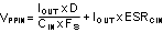
where
- VPPIN : Estimated peak-to-peak input ripple voltage
- IOUT : Output current
- CIN : Input capacitor value
- ESRIN Input capacitor ESR
This capacitor is exposed to significant RMS current, so it is important to select a capacitor with an adequate RMS current rating. Capacitor RMS current estimated as follows:
where
- IRMSCIN Estimated input capacitor RMS current
9.2.3 Application Performance Plots
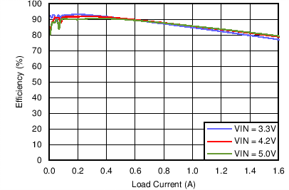 Figure 14. Efficiency Buck 1
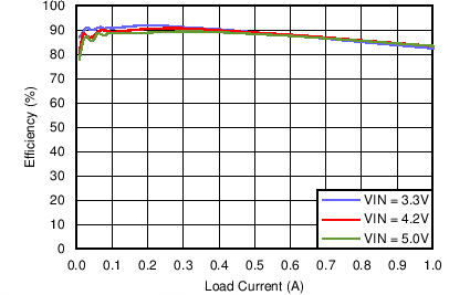 Figure 16. Efficiency Buck 3
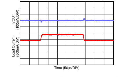 Figure 18. Buck 1 Load Transient (800mA to 1.6A)
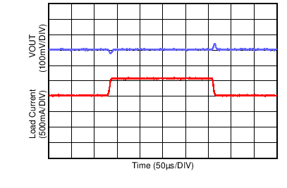 Figure 20. Buck 2 Load Transient (500mA to 1A)
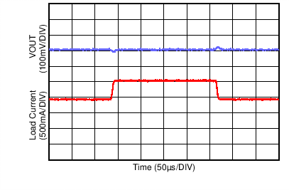 Figure 22. Buck 3 Load Transient (500mA to 1A)
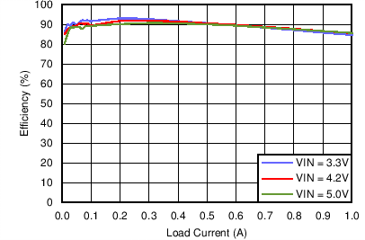 Figure 15. Efficiency Buck 2
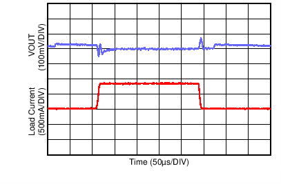 Figure 17. Buck 1 Load Transient (0 to 800mA)
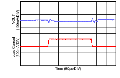 Figure 19. Buck 2 Load Transient (0 to 500mA)
 Figure 21. Buck 3 Load Transient (0 to 500mA)