SNVS999 May 2014 LM10507
PRODUCTION DATA.
- 1 Features
- 2 Applications
- 3 Description
- 4 Simplified Schematic
- 5 Revision History
- 6 Pin Configuration and Functions
-
7 Specifications
- 7.1 Absolute Maximum Ratings
- 7.2 Handling Ratings
- 7.3 Recommended Operating Conditions
- 7.4 Thermal Information
- 7.5 General Electrical Characteristics
- 7.6 Buck 1 Electrical Characteristics
- 7.7 Buck 2 Electrical Characteristics
- 7.8 Buck 3 Electrical Characteristics
- 7.9 LDO Electrical Characteristics
- 7.10 Typical Characteristics
-
8 Detailed Description
- 8.1 Overview
- 8.2 Functional Block Diagram
- 8.3 Feature Description
- 8.4
Device Functional Modes
- 8.4.1 PWM Operation
- 8.4.2 PFM Operation (Bucks 1, 2 & 3)
- 8.4.3 Soft Start
- 8.4.4 Current Limiting
- 8.4.5 Internal Synchronous Rectification
- 8.4.6 Low Dropout Operation
- 8.4.7
Device Operating Modes
- 8.4.7.1 Startup Sequence
- 8.4.7.2 Power-On Default and Device Enable
- 8.4.7.3 RESET: Pin Function
- 8.4.7.4 DEVSLP (Device Sleep) Function
- 8.4.7.5 DEVSLP Terminal
- 8.4.7.6 Device Sleep (DEVSLP) Programming via SPI
- 8.4.7.7 ENABLE, Function
- 8.4.7.8 Under Voltage Lock Out (UVLO)
- 8.4.7.9 Over Voltage Lock Out (OVLO)
- 8.4.7.10 PWR_OK - Pin Function
- 8.4.7.11 Thermal Shutdown (TSD)
- 8.5 Programming
- 8.6 Register Maps
-
9 Applications and Implementation
- 9.1 Application Information
- 9.2
Typical Application
- 9.2.1 Design Requirements
- 9.2.2
Detailed Design Procedure
- 9.2.2.1 Input Voltage
- 9.2.2.2 Output Enable
- 9.2.2.3 Recommendations for Unused Functions and Pins
- 9.2.2.4 External Components Selection
- 9.2.2.5 Output Inductors and Capacitors Selection
- 9.2.2.6 Inductor Selection
- 9.2.2.7 Recommended Method for Inductor Selection
- 9.2.2.8 Alternate Method for Inductor Selection
- 9.2.2.9 Suggested Inductors and Their Suppliers
- 9.2.2.10 Output and Input Capacitors Characteristics
- 9.2.2.11 Output Capacitor Selection
- 9.2.2.12 Input Capacitor Selection
- 9.2.3 Application Performance Plots
- 10Power Supply Recommendations
- 11Layout
- 12Device and Documentation Support
- 13Mechanical, Packaging, and Orderable Information
11 Layout
11.1 Layout Guidelines
PC board layout is an important part of DC-DC converter design. Poor board layout can disrupt the performance of a DC-DC converter and surrounding circuitry by contributing to EMI, ground bounce, and resistive voltage loss in the traces. These can send erroneous signals to the DC-DC converter resulting in poor regulation or instability. Good layout can be implemented by following a few simple design rules.
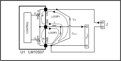 Figure 23. Schematic of LM10507 Highlighting Layout Sensitive Nodes
- Minimize area of switched current loops. In a buck regulator there are two loops where currents are switched rapidly. The first loop starts from the CIN input capacitor, to the regulator VIN terminal, to the regulator SW terminal, to the inductor then out to the output capacitor COUT and load. The second loop starts from the output capacitor ground, to the regulator GND terminals, to the inductor and then out to COUT and the load (see Figure 23). To minimize both loop areas the input capacitor should be placed as close as possible to the VIN terminal. Grounding for both the input and output capacitors should consist of a small localized top side plane that connects to GND. The inductor should be placed as close as possible to the SW pin and output capacitor.
- Minimize the copper area of the switch node. The SW terminals should be directly connected with a trace that runs on top side directly to the inductor. To minimize IR losses this trace should be as short as possible and with a sufficient width. However, a trace that is wider than 100 mils will increase the copper area and cause too much capacitive loading on the SW terminal. The inductors should be placed as close as possible to the SW terminals to further minimize the copper area of the switch node.
- Have a single point ground for all device analog grounds. The ground connections for the feedback components should be connected together then routed to the GND pin of the device. This prevents any switched or load currents from flowing in the analog ground plane. If not properly handled, poor grounding can result in degraded load regulation or erratic switching behavior.
- Minimize trace length to the FB terminal. The feedback trace should be routed away from the SW pin and inductor to avoid contaminating the feedback signal with switch noise.
- Make input and output bus connections as wide as possible. This reduces any voltage drops on the input or output of the converter and can improve efficiency. If voltage accuracy at the load is important make sure feedback voltage sense is made at the load. Doing so will correct for voltage drops at the load and provide the best output accuracy.
11.1.1 PCB Layout Thermal Dissipation for DSBGA Package
- Position ground layer as close as possible to uSMD package. Second PCB layer is usually good option. LM10507 evaluation board is a good example.
- Draw power traces as wide as possible. Bumps which pass through high currents should be connected to wide area this helps the silicon to cool down. Look at LM10507 evaluation board PCB layout for reference
Packaging Information
34 pin uSMD Package, 0.4mm pitch
The dimension for X1, X2 and X3 are as given:
X1 = 2.815 mm + / - 0.030 mm
X2 = 2.815 mm + / - 0.030 mm
X3 = 0.600 mm + / - 0.075 mm
11.2 Layout Example
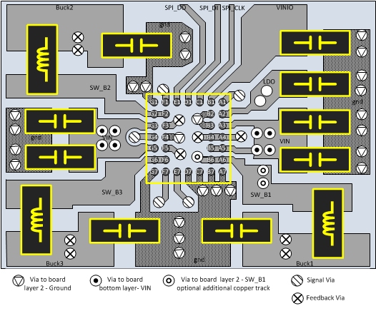 Figure 24. Example of PCB Layout Configuration
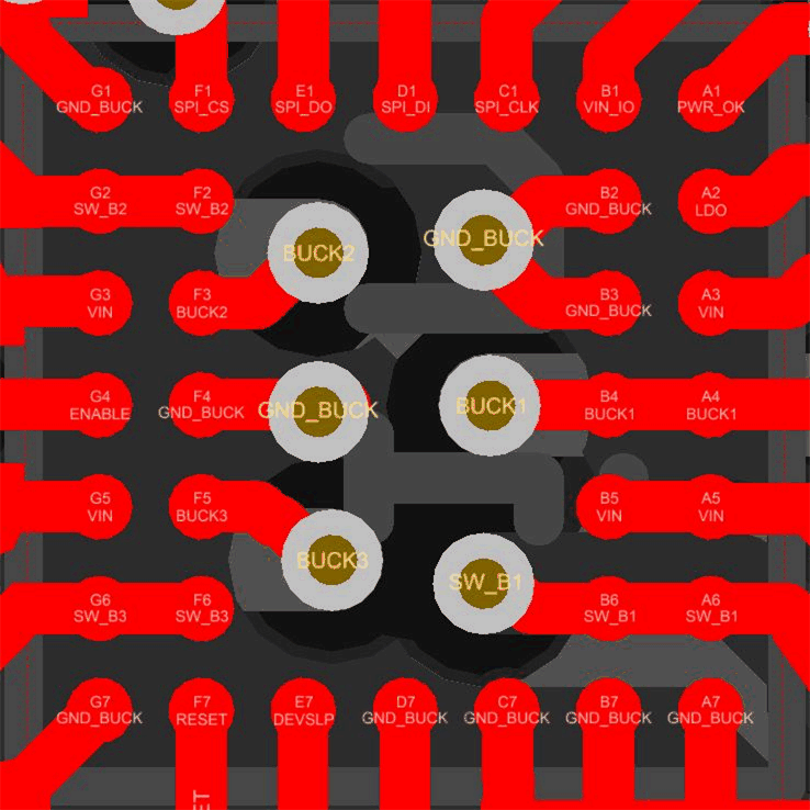 Figure 25. Detail of Device Pins and Centre Vias