SNVS999 May 2014 LM10507
PRODUCTION DATA.
- 1 Features
- 2 Applications
- 3 Description
- 4 Simplified Schematic
- 5 Revision History
- 6 Pin Configuration and Functions
-
7 Specifications
- 7.1 Absolute Maximum Ratings
- 7.2 Handling Ratings
- 7.3 Recommended Operating Conditions
- 7.4 Thermal Information
- 7.5 General Electrical Characteristics
- 7.6 Buck 1 Electrical Characteristics
- 7.7 Buck 2 Electrical Characteristics
- 7.8 Buck 3 Electrical Characteristics
- 7.9 LDO Electrical Characteristics
- 7.10 Typical Characteristics
-
8 Detailed Description
- 8.1 Overview
- 8.2 Functional Block Diagram
- 8.3 Feature Description
- 8.4
Device Functional Modes
- 8.4.1 PWM Operation
- 8.4.2 PFM Operation (Bucks 1, 2 & 3)
- 8.4.3 Soft Start
- 8.4.4 Current Limiting
- 8.4.5 Internal Synchronous Rectification
- 8.4.6 Low Dropout Operation
- 8.4.7
Device Operating Modes
- 8.4.7.1 Startup Sequence
- 8.4.7.2 Power-On Default and Device Enable
- 8.4.7.3 RESET: Pin Function
- 8.4.7.4 DEVSLP (Device Sleep) Function
- 8.4.7.5 DEVSLP Terminal
- 8.4.7.6 Device Sleep (DEVSLP) Programming via SPI
- 8.4.7.7 ENABLE, Function
- 8.4.7.8 Under Voltage Lock Out (UVLO)
- 8.4.7.9 Over Voltage Lock Out (OVLO)
- 8.4.7.10 PWR_OK - Pin Function
- 8.4.7.11 Thermal Shutdown (TSD)
- 8.5 Programming
- 8.6 Register Maps
-
9 Applications and Implementation
- 9.1 Application Information
- 9.2
Typical Application
- 9.2.1 Design Requirements
- 9.2.2
Detailed Design Procedure
- 9.2.2.1 Input Voltage
- 9.2.2.2 Output Enable
- 9.2.2.3 Recommendations for Unused Functions and Pins
- 9.2.2.4 External Components Selection
- 9.2.2.5 Output Inductors and Capacitors Selection
- 9.2.2.6 Inductor Selection
- 9.2.2.7 Recommended Method for Inductor Selection
- 9.2.2.8 Alternate Method for Inductor Selection
- 9.2.2.9 Suggested Inductors and Their Suppliers
- 9.2.2.10 Output and Input Capacitors Characteristics
- 9.2.2.11 Output Capacitor Selection
- 9.2.2.12 Input Capacitor Selection
- 9.2.3 Application Performance Plots
- 10Power Supply Recommendations
- 11Layout
- 12Device and Documentation Support
- 13Mechanical, Packaging, and Orderable Information
6 Pin Configuration and Functions
34 bump DSBGA with 0.4mm pitch
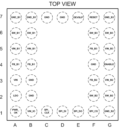
Pin Functions
| Pin | I/O | Description | |
|---|---|---|---|
| Name | No. | ||
| VIN_B1 | A/B5 | I | Buck Switcher Regulator 1 - Power supply voltage input for power stage PFET, if buck 1 is not used, tie to ground to reduce leakage. |
| SW_B1 | A/B6 | O | Buck Switcher Regulator 1 - Power Switching node, connect to inductor |
| FB_B1 | A/B4 | I | Buck Switcher Regulator 1 - Voltage output feedback for Buck Regulator 1 |
| GND_B1 | A/B7 | G | Buck Switcher Regulator 1 - Power ground for Buck Regulator |
| VIN_B2 | G3 | I | Buck Switcher Regulator 2 - Power supply voltage input for power stage PFET, if buck 2 is not used, tie to ground to reduce leakage. |
| SW_B2 | F/G2 | O | Buck Switcher Regulator 2 - Power Switching node, connect to inductor |
| FB_B2 | F3 | I | Buck Switcher Regulator 2 - Voltage output feedback for Buck Regulator 2 |
| GND_B2 | G1 | G | Buck Switcher Regulator 2 - Power ground for Buck Regulator |
| VIN_B3 | G5 | I | Buck Switcher Regulator 3 - Power supply voltage input for power stage PFET |
| SW_B3 | F/G6 | O | Buck Switcher Regulator 3 - Power Switching node, connect to inductor |
| FB_B3 | F5 | I | Buck Switcher Regulator 3 - Voltage output feedback for Buck Regulator 3 |
| GND_B3 | G7 | G | Buck Switcher Regulator 3 - Power ground for Buck Regulator |
| VIN | A3 | I | Power supply Input Voltage, must be present for device to work |
| LDO | A2 | O | LDO Regulator - LDO regulator output voltage |
| SPI_CS | F1 | I | SPI Interface – chip select |
| SPI_DI | D1 | I | SPI Interface – serial data input |
| SPI_DO | E1 | O | SPI Interface – serial data output |
| SPI_CLK | C1 | I | SPI Interface – serial clock input |
| ENABLE | G4 | I | Digital Input Control Signal to Enable/Disable PMIC. Signal Level is related to VIN_IO. This is an active High pin with an internal pull-down resistor. |
| GND | F4 | I | Digital Input Control Signal – Not Used – Connect to GND. |
| DEVSLP | E7 | I | Digital Input Control Signal for entering Device Sleep Mode – see table 1. This is an active High pin with an internal pull-down resistor. |
| RESET | F7 | I | Digital Input Control Signal to abort SPI transactions and resets the PMIC to default Voltages. This is an active Low pin with an internal pull-up resistor. |
| GND | C7 | I | Not Used – Connect to GND. |
| PWR_OK | A1 | O | Digital Output of Power Good signal – all output rails are started. |
| VIN_IO | B1 | P | Supply Voltage for Digital Interface Signals to ASIC like SPI, RESET, DEVSLP, ENABLE, PWR_OK. |
| GND | B2 | G | Ground. Connect to system Ground. |
| GND | B3 | G | Ground. Connect to system Ground. |
| GND | D7 | G | Ground. Connect to system Ground. |
| A: Analog Pin D : Digital Pin G: Ground Pin P: Power Pin I: Input Pin O: Output Pin | |||