SNVS999 May 2014 LM10507
PRODUCTION DATA.
- 1 Features
- 2 Applications
- 3 Description
- 4 Simplified Schematic
- 5 Revision History
- 6 Pin Configuration and Functions
-
7 Specifications
- 7.1 Absolute Maximum Ratings
- 7.2 Handling Ratings
- 7.3 Recommended Operating Conditions
- 7.4 Thermal Information
- 7.5 General Electrical Characteristics
- 7.6 Buck 1 Electrical Characteristics
- 7.7 Buck 2 Electrical Characteristics
- 7.8 Buck 3 Electrical Characteristics
- 7.9 LDO Electrical Characteristics
- 7.10 Typical Characteristics
-
8 Detailed Description
- 8.1 Overview
- 8.2 Functional Block Diagram
- 8.3 Feature Description
- 8.4
Device Functional Modes
- 8.4.1 PWM Operation
- 8.4.2 PFM Operation (Bucks 1, 2 & 3)
- 8.4.3 Soft Start
- 8.4.4 Current Limiting
- 8.4.5 Internal Synchronous Rectification
- 8.4.6 Low Dropout Operation
- 8.4.7
Device Operating Modes
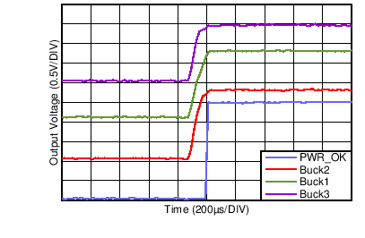
- 8.4.7.1 Startup Sequence
- 8.4.7.2 Power-On Default and Device Enable
- 8.4.7.3 RESET: Pin Function
- 8.4.7.4 DEVSLP (Device Sleep) Function
- 8.4.7.5 DEVSLP Terminal
- 8.4.7.6 Device Sleep (DEVSLP) Programming via SPI
- 8.4.7.7 ENABLE, Function
- 8.4.7.8 Under Voltage Lock Out (UVLO)
- 8.4.7.9 Over Voltage Lock Out (OVLO)
- 8.4.7.10 PWR_OK - Pin Function
- 8.4.7.11 Thermal Shutdown (TSD)
- 8.5 Programming
- 8.6 Register Maps
-
9 Applications and Implementation
- 9.1 Application Information
- 9.2
Typical Application
- 9.2.1 Design Requirements
- 9.2.2
Detailed Design Procedure
- 9.2.2.1 Input Voltage
- 9.2.2.2 Output Enable
- 9.2.2.3 Recommendations for Unused Functions and Pins
- 9.2.2.4 External Components Selection
- 9.2.2.5 Output Inductors and Capacitors Selection
- 9.2.2.6 Inductor Selection
- 9.2.2.7 Recommended Method for Inductor Selection
- 9.2.2.8 Alternate Method for Inductor Selection
- 9.2.2.9 Suggested Inductors and Their Suppliers
- 9.2.2.10 Output and Input Capacitors Characteristics
- 9.2.2.11 Output Capacitor Selection
- 9.2.2.12 Input Capacitor Selection
- 9.2.3 Application Performance Plots
- 10Power Supply Recommendations
- 11Layout
- 12Device and Documentation Support
- 13Mechanical, Packaging, and Orderable Information
7 Specifications
7.1 Absolute Maximum Ratings(1)(2)(3)
| MIN | MAX | UNIT | ||
|---|---|---|---|---|
| VIN, | -0.3 | 6.0 | V | |
| VIN_IO, VIN_B1, VIN_B2, VIN_B3, SPI_CS, SPI_DI, SPI_CLK, SPI_DO, ENABLE, RESET, PWR_OK, DEVSLP | -0.3 | VIN | V | |
| Junction Temperature (TJ-MAX) | 150 | °C | ||
(1) Absolute Maximum Ratings are limits beyond which damage to the device may occur. Operating Ratings are conditions under which operation of the device is ensured. Operating Ratings do not imply ensured performance limits. For ensured performance limits and associated test conditions, see the Electrical Characteristics tables.
(2) Internal thermal shutdown protects device from permanent damage. Thermal shutdown engages at TJ = +140°C and disengages at TJ = +120°C (typ.). Thermal shutdown is ensured by design.
(3) If Military/Aerospace specified devices are required, please contact the Texas Instruments Sales Office/ Distributors for availability and specifications.
7.2 Handling Ratings
| MIN | MAX | UNIT | |||
|---|---|---|---|---|---|
| Tstg | Storage temperature range | -65 | 150 | °C | |
| V(ESD) | Electrostatic discharge | Human body model (HBM), per ANSI/ESDA/JEDEC JS-001, all pins(1) | 1.0 | kV | |
(1) JEDEC document JEP155 states that 500-V HBM allows safe manufacturing with a standard ESD control process.
7.3 Recommended Operating Conditions(1)(2)
over operating free-air temperature range (unless otherwise noted)| MIN | MAX | UNIT | |
|---|---|---|---|
| VIN_B1, VIN_B2_VIN_B3, VIN | 3.0 | 5.5 | V |
| VIN_IO | 1.75 | 3.63, but less than VIN | V |
| Junction Temperature (TJ) | -30 | 125 | °C |
| Ambient Temperature (TA) | -30 | 85 | °C |
| Maximum Continuous Power Dissipation (PD-MAX) (1) | 0.9 | W |
(1) In applications where high power dissipation and/or poor thermal resistance is present the maximum ambient temperature may have to be derated. Maximum ambient temperature (TA-MAX) is dependent on the maximum operating junction temperature (TJ-MAX-OP = +125°C), the maximum power dissipation of the device in the application (PD-MAX), and the junction-to-ambient thermal resistance of the part/package in the application (θJA), as given by the following equation: TA-MAX = TJ-MAX-OP – (θJA × PD-MAX).
(2) The amount of Absolute Maximum power dissipation allowed for the device depends on the ambient temperature and can be calculated using the formula: P = (TJ–TA)/θJA, where TJ is the junction temperature, TA is the ambient temperature, and θJA is the junction-to-ambient thermal resistance. θJA is highly application and board-layout dependent. Internal thermal shutdown circuitry protects the device from permanent damage (see General Electrical Characteristics)
7.4 Thermal Information
| THERMAL METRIC | TYP | UNIT | |||
|---|---|---|---|---|---|
| RθJA | Junction-to-Ambient Thermal Resistance(1) | 44.5 | °C/W | ||
(1) In applications where high power dissipation and/or poor thermal resistance is present the maximum ambient temperature may have to be derated. Maximum ambient temperature (TA-MAX) is dependent on the maximum operating junction temperature (TJ-MAX-OP = +125°C), the maximum power dissipation of the device in the application (PD-MAX), and the junction-to-ambient thermal resistance of the part/package in the application (θJA), as given by the following equation: TA-MAX = TJ-MAX-OP – (θJA × PD-MAX).
7.5 General Electrical Characteristics(1)(2)(4)
| SYMBOL | PARAMETER | TEST CONDITIONS | MIN | TYP | MAX | UNIT |
|---|---|---|---|---|---|---|
| IQ(STANDBY) | Quiescent Supply Current | DEVSLP=High Only Buck3 is ON ,PFM mode, no load. (5) | 50 | 150 | µA | |
| UNDER/OVERVOLTAGE LOCK OUT | ||||||
| VUVLO_RISING | LM10507-A(5) | 2.5 | 2.8 | 2.95 | V | |
| VUVLO_FALLING | (5) | 2.35 | 2.5 | 2.65 | ||
| VOVLO_RISING | LM10507-A(5) | 5.7 | 5.9 | |||
| VOVLO_FALLING | LM10507-A(5) | 5.6 | 5.8 | |||
| DIGITAL INTERFACE | ||||||
| VIL | Logic input low | SPI_CS, SPI_DI, SPI_CLK, ENABLE, RESET, DEVSLP(3)(5) | 0.3*VVIN_IO | V | ||
| VIH | Logic input high | 0.7*VVIN_I0 | ||||
| VOL | Logic output low | PWR_OK (at 2mA load), SPI_DO(5) | 0.2*VVIN_IO | |||
| VOH | Logic output high | 0.8*VVIN_IO | ||||
| IIL | Input current, pindriven low | SPI_CS, SPI_DI, SPI_CLK, ENABLE, DEVSLP | −2 | µA | ||
| RESET | −5 | |||||
| IIH | Input current, pindriven high | SPI_CS, SPI_DI, SPI_CLK, RESET | 2 | µA | ||
| ENABLE, DEVSLP | 5 | |||||
| fSPI_MAX | SPI max frequency | (5) | 10 | MHz | ||
| tDEVSLP | Minimum pulse width (3) | 2 | µs | |||
| tRESET | Minimum pulse width (3) | 2 | µs | |||
| tENABLE | Minimum pulse width (3) | 5 | ||||
| tCOMP | Transition time of PWR_OK output (3) | 0 | 1 | |||
(1) All limits are ensured by design, test and/or statistical analysis. All electrical characteristics having room-temperature limits are tested during production with TJ = 25°C. All hot and cold limits are ensured by correlating the electrical characteristics to process and temperature variations and applying statistical process control.
(2) Capacitors: Low-ESR Surface-Mount Ceramic Capacitors (MLCCs) are used in setting electrical characteristics.
(3) Specification ensured by design. Not tested during production.
(4) Unless otherwise noted, VIN = 5.0V where: VIN = VVIN_B1 = VVIN_B2 = VVIN_B3. Limits apply for TJ = 25°C unless otherwise noted.
(5) Limits apply over the entire operating junction temperature range of −30°C ≤TA = TJ ≤ +85°C.
7.6 Buck 1 Electrical Characteristics(1)(2)(3)(5)
| SYMBOL | PARAMETER | TEST CONDITIONS | MIN | TYP | MAX | UNIT |
|---|---|---|---|---|---|---|
| IQ | DC Bias Current in VIN | No Load, PFM Mode(6) | 15 | 50 | µA | |
| IOUT-MAX | Continuous maximum load current (4)(1)(2) | Buck 1 enabled, switching in PWM (6) | 1.6 | A | ||
| IPEAK | Peak switching current limit | Buck 1 enabled, switching in PWM(6) | 1.9 | 2.2 | 2.8 | A |
| η | Efficiency peak, Buck 1 | IOUT = 0.3A, VVIN = 5.0 V | 90% | |||
| FSW | Switching Frequency(4) | (6) | 1.75 | 2 | 2.3 | MHz |
| CIN | Input Capacitor (4) | 0mA ≤ IOUT ≤ IOUT-MAX | 4.7 | µF | ||
| COUT | Output Filter Capacitor (4) | 10 | 10 | 100 | ||
| Output Capacitor ESR (4) | 20 | mΩ | ||||
| L | Output Filter Inductance (4) | 2.2 | µH | |||
| ΔVOUT | DC Line regulation (4) | 3.3V ≤ VIN ≤ 5.0V, IOUT = IOUT-MAX | 0.5 | %/V | ||
| DC Load regulation, PWM (4) | VVIN=5 V, 0.1 *IOUT-MAX≤ IOUT ≤ IOUT-MAX | 0.3 | %/A | |||
| IFB | Feedback pininput bias current | VFB = 1 V(6) | 1.2 | 5 | µA | |
| VFB | Feedback accuracy | VFB =1 V(6) | -3% | 3% | ||
| RDS-ON-HS | High Side Switch On Resistance | VIN =5.0 V | 135 | mΩ | ||
| VIN = 2.6 V | 215 | |||||
| RDS-ON-LS | Low Side Switch On Resistance | VVIN=5.0 V(6) | 85 | 190 | mΩ | |
| STARTUP | ||||||
| TSTART_NoLoad | Internal soft-start (turn on time) (4) | Startup from shutdown, VOUT = 0V, no load, LC = recommended circuit, using software enable, to VOUT = 95% of final value | 0.1 | ms | ||
| TSTART_FullLoad | Internal soft-start (turn on time) (4) | Startup from shutdown, VOUT = 0V, Maximum Load, LC = recommended circuit, using software enable, to VOUT = 95% of final value | 0.5 | ms | ||
(1) All limits are ensured by design, test and/or statistical analysis. All electrical characteristics having room-temperature limits are tested during production with TJ = 25°C. All hot and cold limits are ensured by correlating the electrical characteristics to process and temperature variations and applying statistical process control.
(2) Capacitors: Low-ESR Surface-Mount Ceramic Capacitors (MLCCs) are used in setting electrical characteristics.
(3) BUCK normal operation is ensured if VIN ≥ VOUT+1.0V.
(4) Specification ensured by design. Not tested during production.
(5) Unless otherwise noted, VIN = 5.0V where: VIN = VVIN_B1 = VVIN_B2 = VVIN_B3. Limits apply for TJ = 25°C unless otherwise noted.
(6) Limits apply over the entire operating junction temperature range of −30°C ≤TA = TJ ≤ +85°C.
7.7 Buck 2 Electrical Characteristics(2)(3)(4)(5)
| SYMBOL | PARAMETER | TEST CONDITIONS | MIN | TYP | MAX | UNIT |
|---|---|---|---|---|---|---|
| IQ | DC Bias Current in VIN | No Load, PFM Mode(6) | 15 | 50 | µA | |
| IOUT -MAX | Continuous maximum load current (1)(1)(2) | Buck 1 enabled, switching in PWM(6) | 1 | A | ||
| IPEAK | Peak switching current limit | Buck 1 enabled, switching in PWM(6) | 1.35 | 1.6 | 1.85 | A |
| η | Efficiency peak, Buck 2 | IOUT = 0.3A, VVIN = 5.0 V | 90% | |||
| FSW | Switching Frequency(1) | (6) | 1.75 | 2 | 2.3 | MHz |
| CIN | Input Capacitor (1) | 0mA ≤ IOUT ≤IOUT-MAX | 4.7 | µF | ||
| COUT | Output Filter Capacitor (1) |
10 | 10 | 100 | ||
| Output Capacitor ESR (1) | 20 | mΩ | ||||
| L | Output Filter Inductance (1) | 2.2 | µH | |||
| ΔVOUT | DC Line regulation (1) | 3.3 V ≤ VIN ≤ 5.0 V, IOUT = IOUT-MAX | 0.5 | %/V | ||
| DC Load regulation (1), PWM | VIN = 5 V, 0.1*IOUT-MAX≤ IOUT ≤ IOUTMAX | 0.3 | %/A | |||
| IFB | Feedback pininput bias current | VFB = 1.8 V(6) | 2.2 | 5 | µA | |
| VFB | Feedback accuracy | VFB = 2 V(6) | -3% | -3% | ||
| RDS-ON-HS | High Side Switch On Resistance | VVIN = 5.0 V | 135 | mΩ | ||
| VIN = 2.6 V | 215 | |||||
| RDS-ON-LS | Low Side Switch On Resistance | VVIN = 5.0 V(6) | 85 | 190 | ||
| STARTUP | ||||||
| TSTART_NoLoad | Internal soft-start (turn on time) (1) | Startup from shutdown, VOUT = 0V, no load, LC = recommended circuit, using software enable, to VOUT = 95% of final value | 0.1 | ms | ||
| TSTART_FullLoad | Internal soft-start (turn on time) (1) | Start up from shutdown, VOUT =0V, Maximum Load, LC = recommended circuit, using software enable, to VOUT = 95% of final value | 0.5 | ms | ||
(1) Specification ensured by design. Not tested during production.
(2) All limits are ensured by design, test and/or statistical analysis. All electrical characteristics having room-temperature limits are tested during production with TJ = 25°C. All hot and cold limits are ensured by correlating the electrical characteristics to process and temperature variations and applying statistical process control.
(3) Capacitors: Low-ESR Surface-Mount Ceramic Capacitors (MLCCs) are used in setting electrical characteristics.
(4) BUCK normal operation is ensured if VIN ≥ VOUT+1.0V.
(5) Unless otherwise noted, VIN = 5.0V where: VIN = VVIN_B1 = VVIN_B2 = VVIN_B3. Limits apply for TJ = 25°C unless otherwise noted.
(6) Limits apply over the entire operating junction temperature range of −30°C ≤TA = TJ ≤ +85°C.
7.8 Buck 3 Electrical Characteristics(2)(3)(4)(5)
| SYMBOL | PARAMETER | TEST CONDITIONS | MIN | TYP | MAX | UNIT |
|---|---|---|---|---|---|---|
| IQ | DC Bias Current in VIN | No Load, PFM Mode(6) | 15 | 50 | µA | |
| IOUT-MAX | Continuous maximum load current(1)(1)(2) | Buck 1 enabled, switching in PWM (6) | 1 | A | ||
| IPEAK | Peak switching current limit | Buck 1 enabled, switching in PWM(6) | 1.35 | 1.6 | 1.85 | A |
| η | Efficiency peak, Buck 3 (1) | IOUT = 0.3A, VVIN=5.0 V | 90% | |||
| FSW | Switching Frequency(1) | (6) | 1.75 | 2 | 2.3 | MHz |
| CIN | Input Capacitor (1) | 0mA ≤ IOUT ≤ IOUT-MAX | 4.7 | µF | ||
| COUT | Output Filter Capacitor (1) | 10 | 10 | 100 | ||
| Output Capacitor ESR (1) | 20 | mΩ | ||||
| L | Output Filter Inductance (1) | 2.2 | µH | |||
| ΔVOUT | DC Line regulation (1) | 3.3 V ≤ VIN ≤ 5.0 V, IOUT = IOUT-MAX | 0.5 | %/V | ||
| DC Load regulation, PWM (1) | VIN=5 V, 0.1* IOUT-MAX ≤ IOUT≥IOUT-MAX | 0.3 | %/A | |||
| IFB | Feedback pininput bias current | VFB = 1.5 V(6) | 1.0 | 5 | µA | |
| VFB | Feedback accuracy | VFB = 3 V (6) | -3% | -3% | ||
| RDS-ON-HS | High Side Switch On Resistance | VVIN=5.0 V | 135 | mΩ | ||
| VIN = 2.6 V | 215 | |||||
| RDS-ON-LS | Low Side Switch On Resistance | VVIN=5.0 V(6) | 85 | 190 | ||
| STARTUP | ||||||
| TSTART_NoLoad | Internal soft-start (turn on time) (1) | Startup from shutdown, VOUT = 0 V, no load, LC = recommended circuit, using software enable, to VOUT = 95% of final value | 0.1 | ms | ||
| TSTART_FullLoad | Internal soft-start (turn on time) (1) | Start up from shutdown, VOUT=0 V, Maximum Load, LC = recommended circuit, using software enable, to VOUT = 95% of final value | 0.5 | ms | ||
(1) Specification ensured by design. Not tested during production.
(2) All limits are ensured by design, test and/or statistical analysis. All electrical characteristics having room-temperature limits are tested during production with TJ = 25°C. All hot and cold limits are ensured by correlating the electrical characteristics to process and temperature variations and applying statistical process control.
(3) Capacitors: Low-ESR Surface-Mount Ceramic Capacitors (MLCCs) are used in setting electrical characteristics.
(4) BUCK normal operation is ensured if VIN ≥ VOUT+1.0 V.
(5) Unless otherwise noted, VIN = 5.0V where: VIN = VVIN_B1 = VVIN_B2 = VVIN_B3. Limits apply for TJ = 25°C unless otherwise noted.
(6) Limits apply over the entire operating junction temperature range of −30°C ≤TA = TJ ≤ +85°C.
7.9 LDO Electrical Characteristics(1)(2)(4)
| SYMBOL | PARAMETER | TEST CONDITIONS | MIN | TYP | MAX | UNIT | |
|---|---|---|---|---|---|---|---|
| VOUT | Output Voltage Accuracy | IOUT = 1mA, VOUT= 2.5 V(5) | −3% | +3% | |||
| IOUT | Maximum Output Current | (5) | 250 | mA | |||
| ISC | Short-Circuit Current Limit | 0.5 | A | ||||
| VDO | Dropout Voltage(3) | IOUT = 250 mA(5) | 200 | 260 | mV | ||
| ΔVOUT | Line Regulation | 3.3 V ≤ VIN ≤ 5.5 V, IOUT = 1mA | 5 | ||||
| Load Regulation | 1mA ≤ IOUT ≤ 250 mA, VIN = 3.3 V, 5.0 V | 5 | |||||
| eN | Output Noise Voltage (3) | 10 Hz ≤ f ≤ 100 kHz | VIN = 5.0 V | 10 | µVRMS | ||
| VIN = 3.3 V | 35 | ||||||
| PSRR | Power Supply Rejection Ratio (3) | F = 10 kHz, COUT = 4.7 µF, IOUT = 20 mA |
VIN = 5.0 V | 65 | dB | ||
| VIN = 3.3 V | 40 | ||||||
| tSTARTUP | Startup Time from Shutdown (3) | COUT = 4.7 µF IOUT = 250mA | VIN = 5.0 V | 45 | µs | ||
| VIN = 3.3 V | 60 | ||||||
| TTRANSIENT | Startup Transient Overshoot (3) | COUT = 4.7 µF IOUT = 250mA(5) | 30 | mV | |||
(1) All limits are ensured by design, test and/or statistical analysis. All electrical characteristics having room-temperature limits are tested during production with TJ = 25°C. All hot and cold limits are ensured by correlating the electrical characteristics to process and temperature variations and applying statistical process control.
(2) Capacitors: Low-ESR Surface-Mount Ceramic Capacitors (MLCCs) are used in setting electrical characteristics.
(3) Dropout voltage is the voltage difference between the input and the output at which the output voltage drops to 100 mV below its nominal value.
(4) Unless otherwise noted, VIN = 5.0V where: VIN = VVIN_B1 = VVIN_B2 = VVIN_B3. Limits apply for TJ = 25°C unless otherwise noted.
(5) Limits apply over the entire operating junction temperature range of −30°C ≤TA = TJ ≤ +85°C.
7.10 Typical Characteristics