JAJSDB4 June   2017 LM193-MIL

PRODUCTION DATA.  

  1. 特長
  2. アプリケーション
  3. 概要
  4. 改訂履歴
  5. Pin Configuration and Functions
  6. Specifications
    1. 6.1 Absolute Maximum Ratings
    2. 6.2 ESD Ratings
    3. 6.3 Recommended Operating Conditions
    4. 6.4 Thermal Information
    5. 6.5 Electrical Characteristics
    6. 6.6 Switching Characteristics
    7. 6.7 Typical Characteristics
  7. Detailed Description
    1. 7.1 Overview
    2. 7.2 Functional Block Diagram
    3. 7.3 Feature Description
    4. 7.4 Device Functional Modes
      1. 7.4.1 Voltage Comparison
  8. Application and Implementation
    1. 8.1 Application Information
    2. 8.2 Typical Application
      1. 8.2.1 Design Requirements
      2. 8.2.2 Detailed Design Procedure
        1. 8.2.2.1 Input Voltage Range
        2. 8.2.2.2 Minimum Overdrive Voltage
        3. 8.2.2.3 Output and Drive Current
        4. 8.2.2.4 Response Time
      3. 8.2.3 Application Curves
  9. Power Supply Recommendations
  10. 10Layout
    1. 10.1 Layout Guidelines
    2. 10.2 Layout Example
  11. 11デバイスおよびドキュメントのサポート
    1. 11.1 関連リンク
    2. 11.2 ドキュメントの更新通知を受け取る方法
    3. 11.3 コミュニティ・リソース
    4. 11.4 商標
    5. 11.5 静電気放電に関する注意事項
    6. 11.6 Glossary
  12. 12メカニカル、パッケージ、および注文情報

パッケージ・オプション

メカニカル・データ(パッケージ|ピン)
サーマルパッド・メカニカル・データ
発注情報

Pin Configuration and Functions

D, JG
8-Pin SOIC, CDIP
Top View
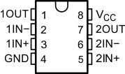
LM193-MIL po_lcs005.gif
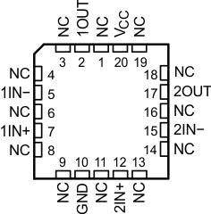
FK Package
20-Pin LCCC
Top View
LM193-MIL po_1_lcs005.gif
NC – No internal connection

Pin Functions

PIN I/O DESCRIPTION
NAME SOIC, CDIP LCCC
1OUT 1 2 Output Output pin of comparator 1
1IN– 2 5 Input Negative input pin of comparator 1
1IN+ 3 7 Input Positive input pin of comparator 1
GND 4 10 Ground
2IN+ 5 12 Input Positive input pin of comparator 2
2IN- 6 15 Input Negative input pin of comparator 2
2OUT 7 17 Output Output pin of comparator 2
VCC 8 20 Supply Pin
NC 1 N/A No Connect (No Internal Connection)
3
4
6
8
9
11
13
14
16
18
19