JAJSBH3D March   2011  – May 2019 LM21215A

PRODUCTION DATA.  

  1. 特長
  2. アプリケーション
    1.     2.5V、500kHz での効率
  3. 概要
    1.     代表的なアプリケーション回路
      1.      Device Images
  4. 改訂履歴
  5. Pin Configuration and Functions
    1.     Pin Functions
  6. Specifications
    1. 6.1 Absolute Maximum Ratings
    2. 6.2 ESD Ratings
    3. 6.3 Recommended Operating Conditions
    4. 6.4 Thermal Information
    5. 6.5 Electrical Characteristics
    6. 6.6 Typical Characteristics
  7. Detailed Description
    1. 7.1 Overview
    2. 7.2 Functional Block Diagram
    3. 7.3 Feature Description
      1. 7.3.1 Precision Enable
      2. 7.3.2 Input Voltage UVLO
      3. 7.3.3 Soft-Start Capability
      4. 7.3.4 PGOOD Indicator
      5. 7.3.5 Frequency Synchronization
      6. 7.3.6 Current Limit
      7. 7.3.7 Short Circuit Protection
    4. 7.4 Device Functional Modes
      1. 7.4.1 Light-Load Operation
      2. 7.4.2 Overvoltage and Undervoltage Handling
      3. 7.4.3 Thermal Shutdown
  8. Application and Implementation
    1. 8.1 Application Information
    2. 8.2 Typical Applications
      1. 8.2.1 Typical Application 1
        1. 8.2.1.1 Design Requirements
        2. 8.2.1.2 Detailed Design Procedure
          1. 8.2.1.2.1 Custom Design With WEBENCH® Tools
          2. 8.2.1.2.2 Output Voltage Setpoint
          3. 8.2.1.2.3 Precision Enable
          4. 8.2.1.2.4 Filter Inductor Selection
          5. 8.2.1.2.5 Output Capacitor Selection
          6. 8.2.1.2.6 Input Capacitor Selection
          7. 8.2.1.2.7 Control Loop Compensation
        3. 8.2.1.3 Application Curves
      2. 8.2.2 Typical Application 2
        1. 8.2.2.1 Design Requirements
        2. 8.2.2.2 Detailed Design Procedure
  9. Power Supply Recommendations
  10. 10Layout
    1. 10.1 Layout Guidelines
      1. 10.1.1 Compact PCB Layout for EMI Reduction
      2. 10.1.2 Thermal Design
      3. 10.1.3 Ground Plane Design
    2. 10.2 Layout Example
  11. 11概要(続き)
  12. 12デバイスおよびドキュメントのサポート
    1. 12.1 デバイス・サポート
      1. 12.1.1 デベロッパー・ネットワークの製品に関する免責事項
      2. 12.1.2 開発サポート
        1. 12.1.2.1 WEBENCH® ツールによるカスタム設計
    2. 12.2 ドキュメントのサポート
      1. 12.2.1 関連資料
    3. 12.3 コミュニティ・リソース
    4. 12.4 商標
    5. 12.5 静電気放電に関する注意事項
    6. 12.6 Glossary
  13. 13メカニカル、パッケージ、および注文情報

パッケージ・オプション

メカニカル・データ(パッケージ|ピン)
サーマルパッド・メカニカル・データ
発注情報

Current Limit

The LM21215A has overcurrent protection to avoid excessive current levels through the power MOSFETs and inductor. A current limit condition exists when the high-side MOSFET's current exceeds the rising current limit level, ICLR. The control circuitry responds to this event by turning off the high-side MOSFET and turning on the low-side MOSFET. This forces a negative voltage on the inductor, thereby causing the inductor current to decrease. The high-side MOSFET does not conduct again until the lower current limit level, ICLF, is sensed on the low-side MOSFET. At this point, the LM21215A resumes normal switching.

A current limit condition causes the internal soft-start voltage to ramp downward. After the internal soft-start ramps below the feedback (FB) voltage, nominally 0.6 V, FB begins to ramp downward, as well. This voltage foldback limits the power consumption in the device during a sustained overload. After the current limit condition is cleared, the internal soft-start voltage ramps up again. Figure 26 describes current limit behavior including VSS, VFB, VOUT and VSW waveforms.
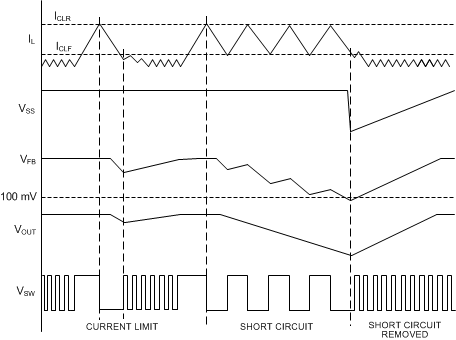
LM21215A current_limit_nosb87.gifFigure 26. Current Limit Conditions