JAJSB11H April 2009 – November 2014 LM25011 , LM25011-Q1
PRODUCTION DATA.
- 1 特長
- 2 アプリケーション
- 3 概要
- 4 改訂履歴
- 5 Pin Configuration and Functions
- 6 Specifications
- 7 Detailed Description
- 8 Application and Implementation
- 9 Power Supply Recommendations
- 10Layout
- 11デバイスおよびドキュメントのサポート
- 12メカニカル、パッケージ、および注文情報
パッケージ・オプション
メカニカル・データ(パッケージ|ピン)
- DGQ|10
サーマルパッド・メカニカル・データ
- DGQ|10
発注情報
5 Pin Configuration and Functions
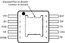
10-Pin
HVSSOP Package
Top View

Pin Functions
| PIN | I/O | DESCRIPTION | APPLICATION INFORMATION | |
|---|---|---|---|---|
| NUMBER | NAME | |||
| 1 | VIN | I | Input supply voltage | Operating input range is 6 V to 42 V. Transient capability is 45 V. A low ESR capacitor must be placed as close as possible to the VIN and SGND pins. |
| 2 | RT | I | On-time Control | An external resistor from VIN to this pin sets the buck switch on-time and the switching frequency. |
| 3 | PGD | – | Power Good | Logic output indicates when the voltage at the FB pin has increased to above 95% of the internal reference voltage. Hysteresis is provided. An external pull-up resistor to a voltage less than 7 V is required. |
| 4 | SS | I | Soft-Start | An internal current source charges an external capacitor to provide the soft-start function. |
| 5 | SGND | Signal Ground | Ground for all internal circuitry other than the current limit sense circuit. | |
| 6 | FB | I | Feedback | Internally connected to the regulation comparator. The regulation level is 2.51 V. |
| 7 | CSG | – | Current Sense Ground | Ground connection for the current limit sensing circuit. Connect to ground and to the current sense resistor. |
| 8 | CS | I | Current sense | Connect to the current sense resistor and the anode of the free-wheeling diode. |
| 9 | SW | O | Switching Node | Internally connected to the buck switch source. Connect to the external inductor, cathode of the free-wheeling diode, and bootstrap capacitor. |
| 10 | BST | I | Bootstrap capacitor connection of the buck switch gate driver. | Connect a 0.1-µF capacitor from SW to this pin. The capacitor is charged during the buck switch off-time via an internal diode. |
| - | EP | – | Exposed Pad | Exposed pad on the underside of the package. This pad should be soldered to the PC board ground plane to aid in heat dissipation. |