JAJSB11H April 2009 – November 2014 LM25011 , LM25011-Q1
PRODUCTION DATA.
- 1 特長
- 2 アプリケーション
- 3 概要
- 4 改訂履歴
- 5 Pin Configuration and Functions
- 6 Specifications
- 7 Detailed Description
- 8 Application and Implementation
- 9 Power Supply Recommendations
- 10Layout
- 11デバイスおよびドキュメントのサポート
- 12メカニカル、パッケージ、および注文情報
パッケージ・オプション
メカニカル・データ(パッケージ|ピン)
- DGQ|10
サーマルパッド・メカニカル・データ
- DGQ|10
発注情報
7.3.3 Current Limit
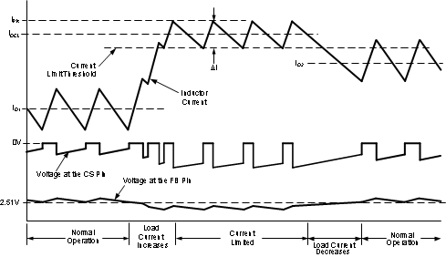
Current limit detection occurs during the off-time by monitoring the voltage across the external current sense resistor RS. Referring to the Functional Block Diagram, during the off-time the recirculating current flows through the inductor, through the load, through the sense resistor, and through D1 to the inductor. If the voltage across the sense resistor exceeds the threshold (VILIM), the current limit comparator output switches to delay the start of the next on-time period. The next on-time starts when the recirculating current decreases such that the voltage across RS reduces to the threshold and the voltage at FB is below 2.51 V. The operating frequency is typically lower due to longer-than-normal off-times. When current limit is detected, the on-time is reduced by approximately 40% (only in LM25011) if the voltage at the FB pin is below its threshold when the voltage across RS reduces to its threshold (VOUT is low due to current limiting).
Figure 15 illustrates the inductor current waveform during normal operation and in current limit. During the first normal operation, the load current is I01, the average of the inductor current waveform. As the load resistance is reduced, the inductor current increases until the lower peak of the inductor ripple current exceeds the threshold. During the current limited portion of Figure 15, each on-time is reduced by approximately 40%, resulting in lower ripple amplitude for the inductor current. During this time the LM25011 is in a constant-current mode with an average load current equal to the current limit threshold plus half the ripple amplitude (IOCL), and the output voltage is below the normal regulated value. Normal operation resumes when the load current is reduced (to IO2), allowing VOUT and the on-time to return to their normal values. Note that in the second period of normal operation, even though the peak current of the inductor exceeds the current limit threshold during part of each cycle, the circuit is not in current limit because the inductor current falls below the current limit threshold during each off-time. The peak current allowed through the buck switch is 3.5 A and the maximum allowed average current is 2.0 A.
 Figure 15. Normal and Current Limit Operation