JAJSAS9F April 2007 – November 2023 LM25116
PRODUCTION DATA
- 1
- 1 特長
- 2 アプリケーション
- 3 概要
- 4 Pin Configuration and Functions
- 5 Specifications
- 6 Detailed Description
-
7 Application and Implementation
- 7.1 Application Information
- 7.2
Typical Application
- 7.2.1 Design Requirements
- 7.2.2
Detailed Design Procedure
- 7.2.2.1 Timing Resistor
- 7.2.2.2 Output Inductor
- 7.2.2.3 Current Sense Resistor
- 7.2.2.4 Ramp Capacitor
- 7.2.2.5 Output Capacitors
- 7.2.2.6 Input Capacitors
- 7.2.2.7 VCC Capacitor
- 7.2.2.8 Bootstrap Capacitor
- 7.2.2.9 Soft Start Capacitor
- 7.2.2.10 Output Voltage Divider
- 7.2.2.11 UVLO Divider
- 7.2.2.12 MOSFETs
- 7.2.2.13 MOSFET Snubber
- 7.2.2.14 Error Amplifier Compensation
- 7.2.2.15 Comprehensive Equations
- 7.2.3 Application Curves
- 7.3 Power Supply Recommendations
- 7.4 Layout
- 8 Device and Documentation Support
- 9 Revision History
- 10Mechanical, Packaging, and Orderable Information
パッケージ・オプション
メカニカル・データ(パッケージ|ピン)
- PWP|20
サーマルパッド・メカニカル・データ
- PWP|20
発注情報
6.3.6 Ramp Generator
The ramp signal used in the pulse width modulator for current mode control is typically derived directly from the buck switch current. This switch current corresponds to the positive slope portion of the inductor current. Using this signal for the PWM ramp simplifies the control loop transfer function to a single pole response and provides inherent input voltage feedforward compensation. The disadvantage of using the buck switch current signal for PWM control is the large leading edge spike due to circuit parasitics that must be filtered or blanked. Also, the current measurement may introduce significant propagation delays. The filtering, blanking time and propagation delay limit the minimal achievable pulse width. In applications where the input voltage may be relatively large in comparison to the output voltage, controlling small pulse widths and duty cycles is necessary for regulation. The LM25116 uses a unique ramp generator which does not actually measure the buck switch current but rather reconstructs the signal. Representing or emulating the inductor current provides a ramp signal to the PWM comparator that is free of leading edge spikes and measurement or filtering delays. The current reconstruction is comprised of two elements, a sample-and-hold DC level and an emulated current ramp.
 Figure 6-5 Composition of Current Sense Signal
The sample-and-hold DC level is derived from a measurement of the recirculating current through either the low-side MOSFET or current sense resistor. The voltage level across the MOSFET or sense resistor is sampled and held just prior to the onset of the next conduction interval of the buck switch. The current sensing and sample-and-hold provide the DC level of the reconstructed current signal. The positive slope inductor current ramp is emulated by an external capacitor connected from the RAMP pin to the AGND and an internal voltage controlled current source. The ramp current source that emulates the inductor current is a function of the VIN and VOUT voltages per Equation 2.
Proper selection of the RAMP capacitor (CRAMP) depends upon the value of the output inductor (L) and the current sense resistor (RS). For proper current emulation, the DC sample and hold value and the ramp amplitude must have the same dependence on the load current. That is in Equation 3.

where
- gm is the ramp generator transconductance (5 µA/V)
- A is the current sense amplifier gain (10 V/V).
The ramp capacitor must be placed very close to the device and connected directly to the pins of the IC (RAMP and AGND).
The difference between the average inductor current and the DC value of the sampled inductor current can cause instability for certain operating conditions. This instability is known as subharmonic oscillation, which occurs when the inductor ripple current does not return to its initial value by the start of next switching cycle. Subharmonic oscillation is normally characterized by observing alternating wide and narrow pulses at the switch node. Adding a fixed slope voltage ramp (slope compensation) to the current sense signal prevents this oscillation. The 25 µA of offset current provided from the emulated current source adds the optimal slope compensation to the ramp signal for a 5-V output. For higher output voltages, additional slope compensation may be required. In these applications, a resistor is added between RAMP and VCC to increase the ramp slope compensation.
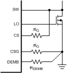
 Figure 6-6 RDS(ON) Current Sensing without Diode Emulation
The DC current sample is obtained using the CS and CSG pins connected to either a source sense resistor (RS) or the RDS(ON) of the low-side MOSFET. For RDS(ON) sensing, RS = RDS(ON) of the low-side MOSFET. In this case it is sometimes helpful to adjust the current sense amplifier gain (A) to a lower value to obtain the desired current limit. Adding external resistors RG in series with CS and CSG, the current sense amplifier gain A becomes Equation 4.
