JAJSCY9 March 2017 LM25141
PRODUCTION DATA.
- 1 特長
- 2 アプリケーション
- 3 概要
- 4 改訂履歴
- 5 Pin Configuration and Functions
- 6 Specifications
-
7 Detailed Description
- 7.1 Overview
- 7.2 Functional Block Diagram
- 7.3
Feature Description
- 7.3.1 High Voltage Start-up Regulator
- 7.3.2 VCC Regulator
- 7.3.3 Oscillator
- 7.3.4 Synchronization
- 7.3.5 Frequency Dithering (Spread Spectrum)
- 7.3.6 Enable
- 7.3.7 Power Good
- 7.3.8 Output Voltage
- 7.3.9 Current Sense
- 7.3.10 DCR Current Sensing
- 7.3.11 Error Amplifier and PWM Comparator
- 7.3.12 Slope Compensation
- 7.3.13 Hiccup Mode Current Limiting
- 7.3.14 Standby Mode
- 7.3.15 Soft-Start
- 7.3.16 Diode Emulation
- 7.3.17 High and Low Side Drivers
- 8 Application and Implementation
- 9 Power Supply Recommendations
- 10Layout
- 11デバイスおよびドキュメントのサポート
- 12メカニカル、パッケージ、および注文情報
10 Layout
10.1 Layout Guidelines
Careful PCB layout is critical to achieve low EMI and stable power supply operation. Make the high frequency current loops as small as possible, and follow these guidelines of good layout practices:
- Keep the high-current paths short. This is essential for stable, jitter-free operation.
- Keep the power traces and load connections short. This is essential for high efficiency. Using 2 oz or thicker copper can enhance full load efficiency.
- Minimize current-sensing errors by routing CS and VOUT using a kelvin sensing directly across the current sense resistor (RSENSE).
- Route high-speed switching nodes (HB, HO, LO, and SW) away from sensitive analog signals (FB, CS, and VOUT).
10.1.1 Layout Procedure
Place the power components first, with ground terminals adjacent to the low-side FET.
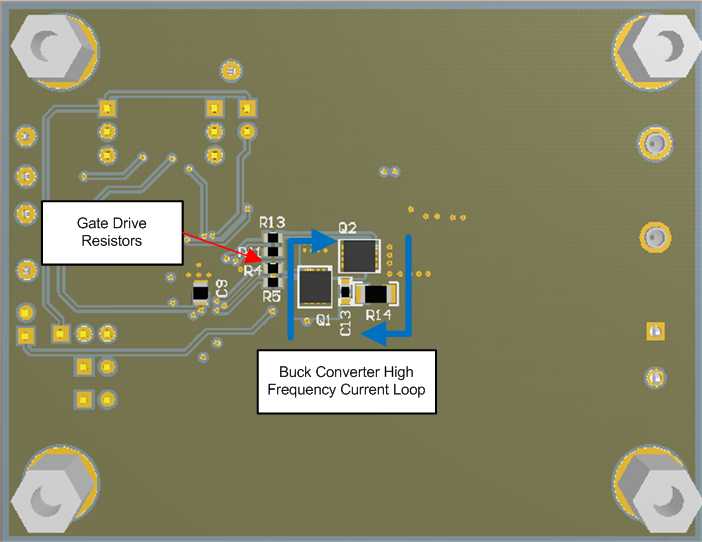
- Mount the controller IC as close as possible to the high and low-side MOSFETs. Make the grounds and high and low-sided drive gate drive lines as short and wide as possible. Place the series gate drive resistor as close to the MOSFET as possible to minimize gate ringing.
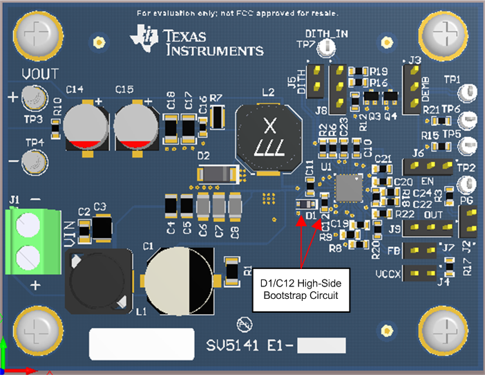
- Locate the gate drive components (D1 and C12) together and near the controller IC; refer to Figure 38. Be aware that peak gate drive currents can be as high as 4 A. Average current up to 75 mA can flow from the VCC pin to the VCC capacitor through the bootstrap diode to the bootstrap capacitor. Size the traces accordingly.
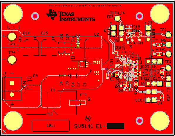
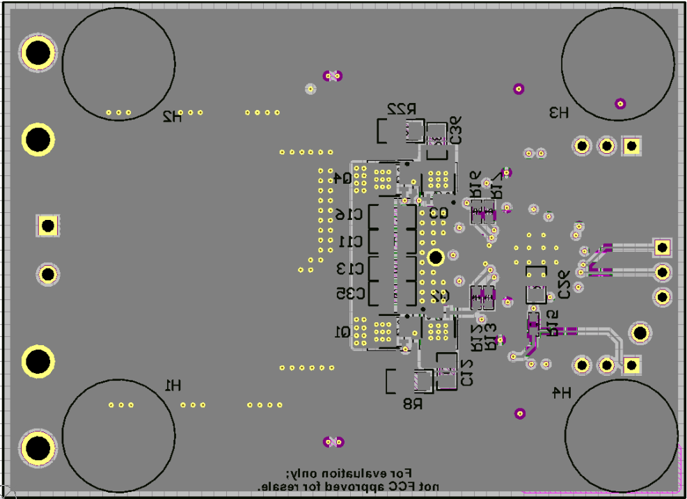
- Figure 39 shows the high frequency loops of the synchronous buck converter. The high frequency current flows through Q1 and Q2, through the power ground plane and back to VIN through the ceramic capacitors C6, C7, and C8. This loop must be as small as possible to minimize EMI. Refer to Figure 41 and Figure 42 for the recommended PCB layout.
- Make the PGND and AGND connections to the LM5141 controller as shown in Figure 40. Create a power grounds directly connected to all high-power components and an analog ground plane for sensitive analog components. The analog ground plane (AGND) and power ground plane (PGND) must be connected at a single point directly under the IC (at the die attach pad or DAP).


