JAJSVG8 October 2024 LM251772
PRODUCTION DATA
- 1
- 1 特長
- 2 アプリケーション
- 3 概要
- 4 Device Comparison
- 5 Pin Configuration and Functions
- 6 Specifications
- 7 Parameter Measurement Information
-
8 Detailed Description
- 8.1 Overview
- 8.2 Functional Block Diagram
- 8.3
Feature Description
- 8.3.1 Buck-Boost Control Scheme
- 8.3.2 Power Save Mode
- 8.3.3 Reference System
- 8.3.4 Supply Voltage Selection – VSMART Switch and Selection Logic
- 8.3.5 Enable and Undervoltage Lockout
- 8.3.6 Internal VCC Regulators
- 8.3.7 Error Amplifier and Control
- 8.3.8 Output Voltage Discharge
- 8.3.9 Peak Current Sensor
- 8.3.10 Short Circuit - Hiccup Protection
- 8.3.11 Current Monitor/Limiter
- 8.3.12 Oscillator Frequency Selection
- 8.3.13 Frequency Synchronization
- 8.3.14 Output Voltage Tracking
- 8.3.15 Slope Compensation
- 8.3.16 Configurable Soft Start
- 8.3.17 Drive Pin
- 8.3.18 Dual Random Spread Spectrum – DRSS
- 8.3.19 Gate Driver
- 8.3.20 Cable Drop Compensation (CDC)
- 8.3.21 CFG-pin and R2D Interface
- 8.3.22 Advanced Monitoring Features
- 8.3.23
Protection Features
- 8.3.23.1 Thermal Shutdown (TSD)
- 8.3.23.2 Over Current Protection
- 8.3.23.3 Output Over Voltage Protection 1 (OVP1)
- 8.3.23.4 Output Over Voltage Protection 2 (OVP2)
- 8.3.23.5 Input Voltage Protection (IVP)
- 8.3.23.6 Input Voltage Regulation (IVR)
- 8.3.23.7 Power Good
- 8.3.23.8 Boot-Strap Under Voltage Protection
- 8.3.23.9 Boot-strap Over Voltage Clamp
- 8.3.23.10 CRC - CHECK
- 8.4 Device Functional Modes
- 8.5 Programming
- 9 LM251772 Registers
-
10Application and Implementation
- 10.1 Application Information
- 10.2
Typical Application
- 10.2.1 Design Requirements
- 10.2.2
Detailed Design Procedure
- 10.2.2.1 Custom Design with WEBENCH Tools
- 10.2.2.2 Frequency
- 10.2.2.3 Feedback Divider
- 10.2.2.4 Inductor and Current Sense Resistor Selection
- 10.2.2.5 Output Capacitor
- 10.2.2.6 Input Capacitor
- 10.2.2.7 Slope Compensation
- 10.2.2.8 UVLO Divider
- 10.2.2.9 Soft-Start Capacitor
- 10.2.2.10 MOSFETs QH1 and QL1
- 10.2.2.11 MOSFETs QH2 and QL2
- 10.2.2.12 Loop Compensation
- 10.2.2.13 External Component Selection
- 10.2.3 Application Curves
- 10.3 Wireless Charging Supply
- 10.4 USB-PD Source with Power Path
- 10.5 Parallel (Multiphase) Operation
- 11Device and Documentation Support
- 12Revision History
- 13Mechanical, Packaging, and Orderable Information
パッケージ・オプション
メカニカル・データ(パッケージ|ピン)
- RHA|40
サーマルパッド・メカニカル・データ
- RHA|40
発注情報
8.3.7.1 Output Voltage Regulation
The device features an internal error amplifier (EA) to regulate the output voltage. The output voltage gets sensed on the FB-pin. The reference for the EA is supplied via the soft-start and VO tracking pins. The COMP-pin is the output of the gm-stage and gets connected to the external compensation network.
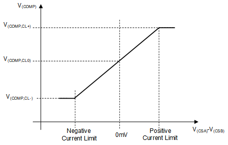
Due to the selected implementation of the error amplifier, the voltage on the LM251772 COMP pin, is in steady-state, accurately reflecting the nominal peak-current value of the inductor.
The Figure 8-16 shoes the control V/I-characteristics of the error amplifier in fPWM mode. You can use this as a guidance for applicative designs where you need to manipulate the inner current loop regulation.

Figure 8-16 Control Function for the Peak Current Sense Voltage Versus VCOMP