JAJSVG8 October 2024 LM251772
PRODUCTION DATA
- 1
- 1 特長
- 2 アプリケーション
- 3 概要
- 4 Device Comparison
- 5 Pin Configuration and Functions
- 6 Specifications
- 7 Parameter Measurement Information
-
8 Detailed Description
- 8.1 Overview
- 8.2 Functional Block Diagram
- 8.3
Feature Description
- 8.3.1 Buck-Boost Control Scheme
- 8.3.2 Power Save Mode
- 8.3.3 Reference System
- 8.3.4 Supply Voltage Selection – VSMART Switch and Selection Logic
- 8.3.5 Enable and Undervoltage Lockout
- 8.3.6 Internal VCC Regulators
- 8.3.7 Error Amplifier and Control
- 8.3.8 Output Voltage Discharge
- 8.3.9 Peak Current Sensor
- 8.3.10 Short Circuit - Hiccup Protection
- 8.3.11 Current Monitor/Limiter
- 8.3.12 Oscillator Frequency Selection
- 8.3.13 Frequency Synchronization
- 8.3.14 Output Voltage Tracking
- 8.3.15 Slope Compensation
- 8.3.16 Configurable Soft Start
- 8.3.17 Drive Pin
- 8.3.18 Dual Random Spread Spectrum – DRSS
- 8.3.19 Gate Driver
- 8.3.20 Cable Drop Compensation (CDC)
- 8.3.21 CFG-pin and R2D Interface
- 8.3.22 Advanced Monitoring Features
- 8.3.23
Protection Features
- 8.3.23.1 Thermal Shutdown (TSD)
- 8.3.23.2 Over Current Protection
- 8.3.23.3 Output Over Voltage Protection 1 (OVP1)
- 8.3.23.4 Output Over Voltage Protection 2 (OVP2)
- 8.3.23.5 Input Voltage Protection (IVP)
- 8.3.23.6 Input Voltage Regulation (IVR)
- 8.3.23.7 Power Good
- 8.3.23.8 Boot-Strap Under Voltage Protection
- 8.3.23.9 Boot-strap Over Voltage Clamp
- 8.3.23.10 CRC - CHECK
- 8.4 Device Functional Modes
- 8.5 Programming
- 9 LM251772 Registers
-
10Application and Implementation
- 10.1 Application Information
- 10.2
Typical Application
- 10.2.1 Design Requirements
- 10.2.2
Detailed Design Procedure
- 10.2.2.1 Custom Design with WEBENCH Tools
- 10.2.2.2 Frequency
- 10.2.2.3 Feedback Divider
- 10.2.2.4 Inductor and Current Sense Resistor Selection
- 10.2.2.5 Output Capacitor
- 10.2.2.6 Input Capacitor
- 10.2.2.7 Slope Compensation
- 10.2.2.8 UVLO Divider
- 10.2.2.9 Soft-Start Capacitor
- 10.2.2.10 MOSFETs QH1 and QL1
- 10.2.2.11 MOSFETs QH2 and QL2
- 10.2.2.12 Loop Compensation
- 10.2.2.13 External Component Selection
- 10.2.3 Application Curves
- 10.3 Wireless Charging Supply
- 10.4 USB-PD Source with Power Path
- 10.5 Parallel (Multiphase) Operation
- 11Device and Documentation Support
- 12Revision History
- 13Mechanical, Packaging, and Orderable Information
パッケージ・オプション
メカニカル・データ(パッケージ|ピン)
- RHA|40
サーマルパッド・メカニカル・データ
- RHA|40
発注情報
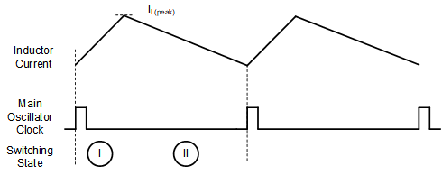
8.3.1.2 Boost Mode
In boost mode operation, the converter starts a boost magnetization cycle (switching state I) with the internal clock signal. After it samples the inductor current, the device transitions to switching state II, which is the boost demagnetization state. The maximum duty cycle in boost mode is limited by the minimum boost on-time and the selected switching frequency.

Figure 8-4 Inductor Current in Continuous Current Boost Operation