SNVS430I May 2006 – March 2015 LM26001 , LM26001-Q1
PRODUCTION DATA.
6 Specifications
6.1 Absolute Maximum Ratings(1)(2)
| MIN | MAX | UNIT | ||
|---|---|---|---|---|
| Voltages from the indicated pins to GND | VIN | –0.3 | 40 | V |
| SW(5) | –0.5 | 40 | V | |
| VDD | –0.3 | 7 | V | |
| VBIAS | –0.3 | 10 | V | |
| FB | –0.3 | 6 | V | |
| BOOT | SW-0.3 | SW+7 | V | |
| PGOOD | –0.3 | 7 | V | |
| FREQ | –0.3 | 7 | V | |
| SYNC | –0.3 | 7 | V | |
| EN | –0.3 | 40 | V | |
| FPWM | –0.3 | y7 | V | |
| SS | –0.3 | 7 | V | |
| Power Dissipation(1)(3) | 2.6 | W | ||
| Recommended Lead Temperature | Vapor Phase (70s) | 215 | °C | |
| Infrared (15s) | 220 | °C | ||
| Storage temperature | Tstg | –65 | 150 | °C |
(1) The maximum allowable power dissipation is a function of the maximum junction temperature, TJ_MAX, the junction-to-ambient thermal resistance, θJA, and the ambient temperature, TA. The maximum allowable power dissipation at any ambient temperature is calculated using: PD_MAX = (TJ_MAX - TA) /θJA. The maximum power dissipation of 2.6W is determined using TA = 25°C, θJA = 38°C/W, and TJ_MAX = 125°C. The number stated here reflects the maximum power dissipation for the package and not the device.
(2) If Military/Aerospace specified devices are required, please contact the Texas Instruments Sales Office/Distributors for availability and specifications.
(3) For Device Power Dissipation, please refer to section 10.3.
6.2 ESD Ratings - LM26001
| VALUE | UNIT | |||
|---|---|---|---|---|
| V(ESD) | Electrostatic discharge | Human body model (HBM), per ANSI/ESDA/JEDEC JS-001, all pins(1) | ± 2 | kV |
| Charged device model (CDM), per JEDEC specification JESD22-C101, all pins(2) | ± 1 | |||
| Machine model | ± 200 | V | ||
(1) JEDEC document JEP155 states that 500-V HBM allows safe manufacturing with a standard ESD control process.
(2) JEDEC document JEP157 states that 250-V CDM allows safe manufacturing with a standard ESD control process.
6.3 ESD Ratings - LM26001-Q1
| VALUE | UNIT | ||||
|---|---|---|---|---|---|
| V(ESD) | Electrostatic discharge | Human body model (HBM), per AEC Q100-002(1) | ± 2 | kV | |
| Charged device model (CDM), per AEC Q100-011 | Corner pins (1, 8, 9, and 16) | ± 1 | |||
| Other pins | ± 1 | ||||
| Machine model | ± 200 | V | |||
(1) AEC Q100-002 indicates HBM stressing is done in accordance with the ANSI/ESDA/JEDEC JS-001 specification.
6.4 Recommended Operating Conditions
over operating free-air temperature range (unless otherwise noted)| MIN | MAX | UNIT | |
|---|---|---|---|
| Operating Junction Temp. | –40 | 125 | °C |
| Supply Voltage(2) | 3.0 | 38 | V |
6.5 Thermal Information
| THERMAL METRIC(1) | LM26001 | UNIT | |
|---|---|---|---|
| PWP | |||
| 16 PINS | |||
| RθJA | Junction-to-ambient thermal resistance | 38.8 | °C/W |
| RθJC(top) | Junction-to-case (top) thermal resistance | 23.0 | |
| RθJB | Junction-to-board thermal resistance | 16.7 | |
| ψJT | Junction-to-top characterization parameter | 0.6 | |
| ψJB | Junction-to-board characterization parameter | 16.4 | |
| RθJC(bot) | Junction-to-case (bottom) thermal resistance | 1.7 | |
(1) For more information about traditional and new thermal metrics, see the IC Package Thermal Metrics application report, SPRA953.
6.6 Electrical Characteristics
Unless otherwise stated, Vin=12 V. Minimum and Maximum limits are ensured through test, design, or statistical correlation. Typical values represent the most likely parametric norm at TJ = 25°C, and are provided for reference purposes only.(3)| PARAMETER | TEST CONDITIONS | MIN | TYP | MAX | UNIT | |
|---|---|---|---|---|---|---|
| SYSTEM | ||||||
| ISD(4) | Shutdown Current | EN = 0 V | 10.8 | µA | ||
| EN = 0 V, –40°C ≤ TJ ≤ 125°C | 20 | |||||
| Iq_Sleep_VB(4) | Quiescent Current | Sleep mode, VBIAS = 5 V | 38 | µA | ||
| Sleep mode, VBIAS = 5 V, –40°C ≤ TJ ≤ 125°C | 70 | |||||
| Iq_Sleep_VDD | Quiescent Current | Sleep mode, VBIAS = GND | 75 | µA | ||
| Sleep mode, VBIAS = GND, –40°C ≤ TJ ≤ 125°C | 125 | |||||
| Iq_PWM_VB | Quiescent Current | PWM mode, VBIAS = 5 V | 150 | 230 | µA | |
| Iq_PWM_VDD | Quiescent Current | PWM mode, VBIAS = GND | 0.65 | 0.85 | mA | |
| IBIAS_Sleep(4) | Bias Current | Sleep mode, VBIAS = 5 V | 33 | µA | ||
| Sleep mode, VBIAS = 5 V, –40°C ≤ TJ ≤ 125°C | 85 | |||||
| IBIAS_PWM | Bias Current | PWM mode, VBIAS = 5 V | 0.5 | 0.70 | mA | |
| VFB | Feedback Voltage | 5 V < Vin < 38 V | 1.234 | V | ||
| 5 V < Vin < 38 V, –40°C ≤ TJ ≤ 125°C | 1.2155 | 1.2525 | ||||
| IFB | FB Bias Current | ±200 | nA | |||
| ΔVOUT/ΔVIN | Vout line regulation | 5 V < Vin < 38 V | 0.001 | %/V | ||
| ΔVOUT/ΔIOUT | Vout load regulation | 0.8 V < VCOMP < 1.15 V | 0.07% | |||
| VDD | VDD output voltage | 7 V < Vin < 35 V, IVDD= 0 mA to 5 mA | 5.95 | V | ||
| 7 V < Vin < 35 V, IVDD= 0 mA to 5 mA, –40°C ≤ TJ ≤ 125°C | 5.50 | 6.50 | ||||
| ISS_Source | Soft-start source current | 2.2 | µA | |||
| –40°C ≤ TJ ≤ 125°C | 1.5 | 4.6 | ||||
| Vbias_th | VBIAS On Voltage | Specified at IBIAS = 92.5% of full value | 2.64 | 2.9 | 3.07 | V |
| SWITCHING | ||||||
| RDS(ON) | Switch on Resistance | Isw = 1A | 0.2 | Ω | ||
| Isw = 1A, –40°C ≤ TJ ≤ 125°C | 0.12 | 0.42 | ||||
| Isw_off | Switch off state leakage current | Vin = 38 V, VSW = 0 V | 0.002 | µA | ||
| Vin = 38 V, VSW = 0 V, –40°C ≤ TJ ≤ 125°C | 5.0 | |||||
| fsw | Switching Frequency | RFREQ = 62k, 124k, 240k | ±10% | |||
| VFREQ | FREQ voltage | 1.0 | V | |||
| fSW range | Switching Frequency range | –40°C ≤ TJ ≤ 125°C | 150 | 500 | kHz | |
| VSYNC | Sync pin threshold | SYNC rising | 1.2 | V | ||
| SYNC rising, –40°C ≤ TJ ≤ 125°C | 1.6 | |||||
| SYNC falling | 1.1 | |||||
| SYNC falling, –40°C ≤ TJ ≤ 125°C | 0.8 | |||||
| Sync pin hysteresis | 114 | mV | ||||
| ISYNC | SYNC leakage current | 6 | nA | |||
| FSYNC_UP | Upper frequency synchronization range | As compared to nominal fSW, –40°C ≤ TJ ≤ 125°C | 30% | |||
| FSYNC_DN | Lower frequency synchronization range | As compared to nominal fSW, –40°C ≤ TJ ≤ 125°C | –20% | |||
| TOFFMIN | Minimum Off-time | 365 | ns | |||
| TONMIN | Minimum On-time | 155 | ns | |||
| THSLEEP_HYS | Sleep mode threshold hysteresis | VFB rising, % of THWAKE | 101.2% | |||
| THWAKE | Wake up threshold | Measured at falling FB, COMP = 0.6 V | 1.234 | V | ||
| IBOOT | BOOT pin leakage current | BOOT = 16 V, SW = 10 V | 0.0006 | µA | ||
| BOOT = 16 V, SW = 10 V, –40°C ≤ TJ ≤ 125°C | 5.0 | |||||
| PROTECTION | ||||||
| ILIMPK | Peak Current Limit | 2.5 | A | |||
| –40°C ≤ TJ ≤ 125°C | 1.85 | 3.2 | ||||
| VFB_SC | Short circuit frequency foldback threshold | Measured at FB falling | 0.87 | V | ||
| F_min_sc | Min Frequency in foldback | VFB < 0.3 V | 71 | kHz | ||
| VTH_PGOOD | Power Good Threshold | Measured at FB, PGOOD rising | 92% | |||
| Measured at FB, PGOOD rising, –40°C ≤ TJ ≤ 125°C | 89% | 95% | ||||
| PGOOD hysteresis | 2% | 7% | 8% | |||
| IPGOOD_HI | PGOOD leakage current | PGOOD = 5 V | 0.2 | nA | ||
| RDS_PGOOD | PGOOD on resistance | PGOOD sink current = 500 µA | 64 | Ω | ||
| VUVLO | Under-voltage Lock-Out Threshold | Vin falling , shutdown, VDD = VIN | 2.9 | V | ||
| Vin falling , shutdown, VDD = VIN, –40°C ≤ TJ ≤ 125°C | 2.60 | 3.20 | ||||
| Vin rising, soft-start, VDD = VIN | 3.9 | |||||
| Vin rising, soft-start, VDD = VIN, –40°C ≤ TJ ≤ 125°C | 3.60 | 4.20 | ||||
| TSD | Thermal Shutdown Threshold | 160 | °C | |||
| θJA | Thermal resistance | Power dissipation = 1W, 0 lfpm air flow | 38 | °C/W | ||
| LOGIC | ||||||
| VthEN | Enable Threshold voltage | 1.2 | V | |||
| –40°C ≤ TJ ≤ 125°C | 0.8 | 1.4 | ||||
| Enable hysteresis | 120 | mV | ||||
| IEN_Source | EN source current | EN = 0 V | 4.5 | µA | ||
| VTH_FPWM | FPWM threshold | 1.2 | V | |||
| –40°C ≤ TJ ≤ 125°C | 0.8 | 1.6 | ||||
| IFPWM | FPWM leakage current | FPWM = 5 V | 35 | nA | ||
| EA | ||||||
| gm | Error amp trans-conductance | 670 | µmho | |||
| –40°C ≤ TJ ≤ 125°C | 400 | 1000 | ||||
| ICOMP | COMP source current | VCOMP = 0.9 V | 56 | µA | ||
| COMP sink current | VCOMP = 0.9 V | 56 | µA | |||
| VCOMP | COMP pin voltage range | 0.64 | 1.27 | V | ||
(1) Absolute Maximum Ratings indicate limits beyond which damage to the device may occur. Recommended Operating Conditions indicate conditions for which the device is intended to be functional, but do not ensure specific performance limits. For ensured specifications and test conditions, see the Electrical Characteristics.
(2) Below 4.0-V input, power dissipation may increase due to increased RDS(ON). Therefore, a minimum input voltage of 4.0 V is required to operate continuously within specification. A minimum of 3.9 V (typical) is also required for startup.
(3) All room temperature limits are 100% production tested. All limits at temperature extremes are ensured through correlation using standard Statistical Quality Control (SQC) methods. All limits are used to calculate Average Outgoing Quality Level (AOQL).
(4) Iq and ISD specify the current into the VIN pin. IBIAS is the current into the VBIAS pin when the VBIAS voltage is greater than 3 V. All quiescent current specifications apply to non-switching operation.
(5) The absolute maximum specification applies to DC voltage. An extended negative voltage limit of -2V applies for a pulse of up to 1 µs, and –1 V for a pulse of up to 20 µs.
6.7 Typical Characteristics
Unless otherwise specified the following conditions apply: VIN = 12 V, TJ = 25°C.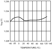 Figure 1. VFB vs Temperature
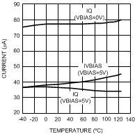 Figure 3. IQ and IVBIAS vs Temperature (Sleep Mode)
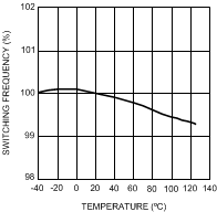 Figure 5. Normalized Switching Frequency vs Temperature (300 kHz)
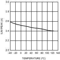 Figure 7. Peak Current Limit vs Temperature
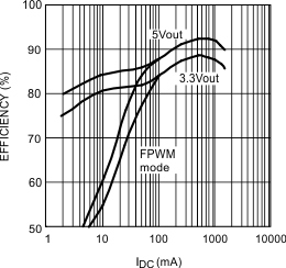 Figure 9. Efficiency vs Load Current (330 kHz)
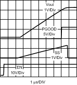 Figure 11. Startup Waveforms
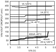 Figure 13. Low Input Voltage Dropout Nominal VOUT = 5 V
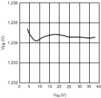 Figure 2. VFB vs Vin (IDC = 300 mA)
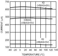 Figure 4. IQ and IVBIAS vs Temperature (PWM Mode)
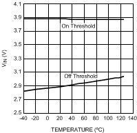 Figure 6. UVLO Threshold vs Temperature (VDD = VIN)
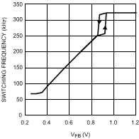 Figure 8. Short Circuit Foldback Frequency vs VFB (325 kHz Nominal)
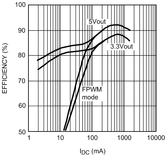 Figure 10. Efficiency vs Load Current (500 kHz)
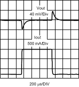 Figure 12. Load Transient Response