JAJSDZ5 October   2017 LM2623-Q1

PRODUCTION DATA.  

  1. 特長
  2. アプリケーション
  3. 概要
    1.     Device Images
      1.      代表的なアプリケーション
  4. 改訂履歴
  5. Pin Configuration and Functions
    1.     Pin Functions
  6. Specifications
    1. 6.1 Absolute Maximum Ratings
    2. 6.2 ESD Ratings
    3. 6.3 Recommended Operating Conditions
    4. 6.4 Thermal Information
    5. 6.5 Electrical Characteristics
    6. 6.6 Typical Characteristics
  7. Detailed Description
    1. 7.1 Overview
    2. 7.2 Functional Block Diagram
    3. 7.3 Feature Description
      1. 7.3.1 Gated Oscillator Control Scheme
      2. 7.3.2 Cycle-To-Cycle PFM
      3. 7.3.3 Shutdown
      4. 7.3.4 Internal Current Limit and Thermal Protection
    4. 7.4 Device Functional Modes
      1. 7.4.1 Pulse Frequency Modulation (PFM)
      2. 7.4.2 Low Voltage Start-Up
  8. Applications and Implementation
    1. 8.1 Application Information
    2. 8.2 Typical Application
      1. 8.2.1 Design Requirements
      2. 8.2.2 Detailed Design Procedure
        1. 8.2.2.1 Non-Linear Effect
        2. 8.2.2.2 Choosing the Correct C3 Capacitor
        3. 8.2.2.3 Setting the Output Voltage
        4. 8.2.2.4 VDD Supply
        5. 8.2.2.5 Setting the Switching Frequency
        6. 8.2.2.6 Output Diode Selection
      3. 8.2.3 Application Curves
  9. Power Supply Recommendations
  10. 10Layout
    1. 10.1 Layout Guidelines
      1. 10.1.1 Boost Output Capacitor Placement
      2. 10.1.2 Schottky Diode Placement
      3. 10.1.3 Boost Input / VDD Capacitor Placement
    2. 10.2 Layout Example
    3. 10.3 WSON Package Devices
  11. 11デバイスおよびドキュメントのサポート
    1. 11.1 デバイス・サポート
      1. 11.1.1 デベロッパー・ネットワークの製品に関する免責事項
    2. 11.2 ドキュメントのサポート
      1. 11.2.1 関連資料
    3. 11.3 ドキュメントの更新通知を受け取る方法
    4. 11.4 コミュニティ・リソース
    5. 11.5 商標
    6. 11.6 静電気放電に関する注意事項
    7. 11.7 Glossary
  12. 12メカニカル、パッケージ、および注文情報

パッケージ・オプション

メカニカル・データ(パッケージ|ピン)
サーマルパッド・メカニカル・データ
発注情報

Gated Oscillator Control Scheme

The on/off regulation mode of the LM2623-Q1, along with its ultra-low quiescent current, results in good efficiency over a very wide load range. The internal oscillator frequency can be programmed using an external resistor to be constant or vary with the battery voltage. Adding a capacitor to program the frequency allows the designer to adjust the duty cycle and optimize it for the application. Adding a resistor in addition to the capacitor allows the duty cycle to dynamically compensate for changes to the input/output voltage ratio. This is called a ratio-adaptive gated-oscillator circuit. See the Typical Application for a sample application circuit. Using the correct RC components to adjust the oscillator allows the device to run with low ripple and high efficiency over a wide range of loads and input/output voltages.
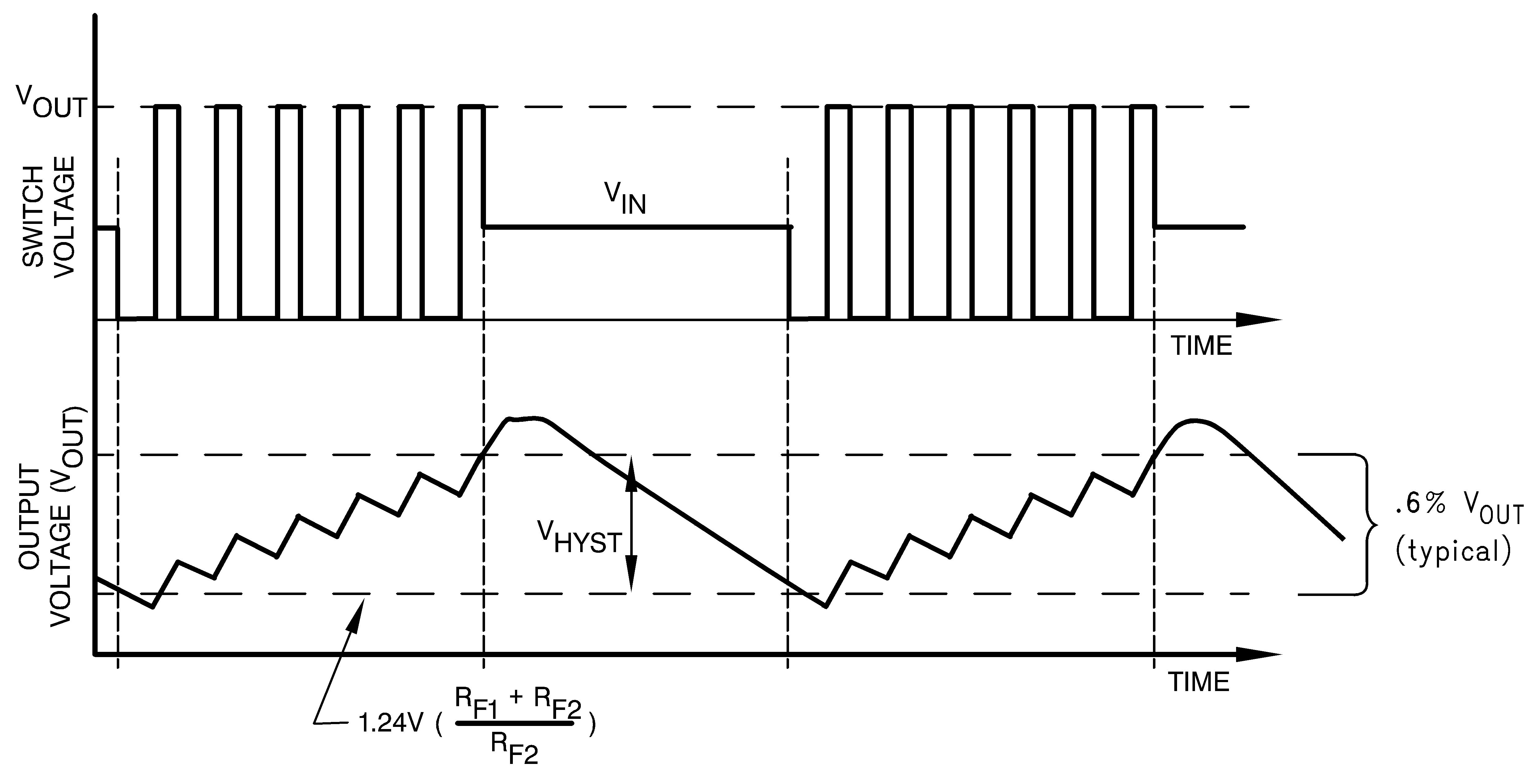
LM2623-Q1 20038815.pngFigure 8. Typical Step-Up Regulator Waveforms