SNVS188I May 2004 – October 2017 LM2623
PRODUCTION DATA.
- 1 Features
- 2 Applications
- 3 Description
- 4 Revision History
- 5 Pin Configuration And Functions
- 6 Specifications
- 7 Detailed Description
- 8 Applications And Implementation
- 9 Power Supply Recommendations
- 10Layout
- 11Device And Documentation Support
- 12Mechanical, Packaging, And Orderable Information
パッケージ・オプション
メカニカル・データ(パッケージ|ピン)
サーマルパッド・メカニカル・データ
発注情報
10 Layout
10.1 Layout Guidelines
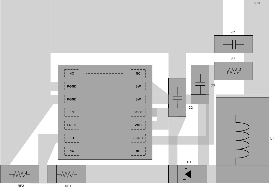
The example layouts below follow proper layout guidelines and should be used as a guide for laying out the LM2623 circuit. The LM2623 inductive boost converter sees a high switched voltage at the SW pin, and a step current through the Schottky diode and output capacitor each switching cycle. The high switching voltage can create interference into nearby nodes due to electric field coupling (I = C x dV/dt). The large step current through the diode and the output capacitor can cause a large voltage spike at the SW and BOOST pins due to parasitic inductance in the step current conducting path (V = L x di/dt). Board layout guidelines are geared towards minimizing this electric field coupling and conducted noise.
Boost Output Capacitor Placement, Schottky Diode Placement, and Boost Input / VDD Capacitor Placement detail the main (layout sensitive) areas of the LM2623 inductive boost converter in order of decreasing importance:
10.1.1 Boost Output Capacitor Placement
Because the output capacitor is in the path of the inductor current discharge path, it will see a high-current step from 0 to IPEAK each time the switch turns off and the Schottky diode turns on. Any inductance along this series path from the diodes cathode, through COUT, and back into the LM2623 GND pin will contribute to voltage spikes at SW. These spikes can potentially over-voltage the SW and BOOST pins, or feed through to GND. To avoid this, COUT+ must be connected as close as possible to the cathode of the Schottky diode, and COUT− must be connected as close as possible to the LM2623 GND bumps. The best placement for COUT is on the same layer as the LM2623 to avoid any vias that can add excessive series inductance.
10.1.2 Schottky Diode Placement
In the LM2623 device boost circuit the Schottky diode is in the path of the inductor current discharge. As a result the Schottky diode sees a high-current step from 0 to IPEAK each time the switch turns off, and the diode turns on. Any inductance in series with the diode will cause a voltage spike at SW. This can potentially over-voltage the SW pin, or feed through to VOUT and through the output capacitor, into GND. Connecting the anode of the diode as close as possible to the SW pin, and connecting the cathode of the diode as close as possible to COUT+, will reduce the inductance (LP_) and minimize these voltage spikes.
10.1.3 Boost Input / VDD Capacitor Placement
The LM2623 input capacitor filters the inductor current ripple and the internal MOSFET driver currents. The inductor current ripple can add input voltage ripple due to any series resistance in the input power path. The MOSFET driver currents can add voltage spikes on the input due to the inductance in series with the VIN/VDD and the input capacitor. Close placement of the input capacitor to the VDD pin and to the GND pin is critical since any series inductance between VIN/VDD and CIN+ or CIN– and GND can create voltage spikes that could appear on the VIN/VDD supply line and GND.
10.2 Layout Example

10.3 WSON Package Devices
The LM2623 is offered in the 14-lead WSON surface mount package to allow for increased power dissipation compared to the VSSOP-8. For details of the thermal performance as well as mounting and soldering specifications, refer to Application Note AN-1187 Leadless Leadframe Package (LLP) (SNOA401).