JAJS908F May 2004 – June 2016 LM2675
PRODUCTION DATA.
- 1 特長
- 2 アプリケーション
- 3 概要
- 4 改訂履歴
- 5 Description (continued)
- 6 Pin Configuration and Functions
-
7 Specifications
- 7.1 Absolute Maximum Ratings
- 7.2 ESD Ratings
- 7.3 Recommended Operating Conditions
- 7.4 Thermal Information
- 7.5 Electrical Characteristics - 3.3 V
- 7.6 Electrical Characteristics - 5 V
- 7.7 Electrical Characteristics - 12 V
- 7.8 Electrical Characteristics - Adjustable
- 7.9 Electrical Characteristics - All Output Voltage Versions
- 7.10 Typical Characteristics
- 7.11 Typical Characteristics - Fixed Output Voltage Versions
- 8 Detailed Description
- 9 Application and Implementation
- 10Power Supply Recommendations
- 11Layout
- 12デバイスおよびドキュメントのサポート
- 13メカニカル、パッケージ、および注文情報
11 Layout
11.1 Layout Guidelines
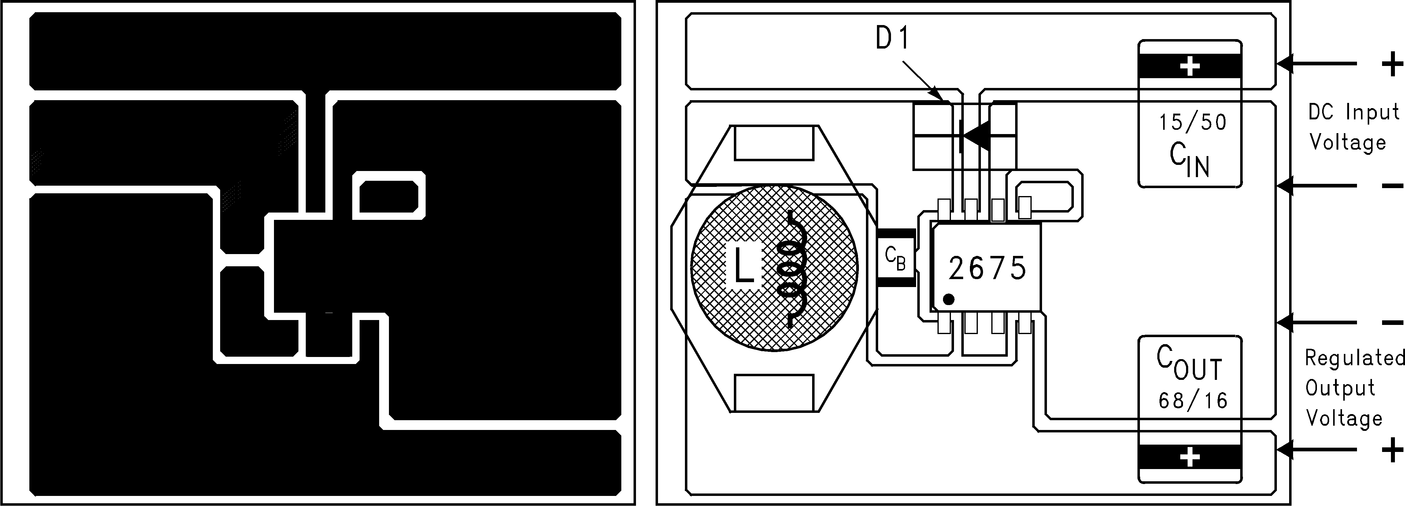
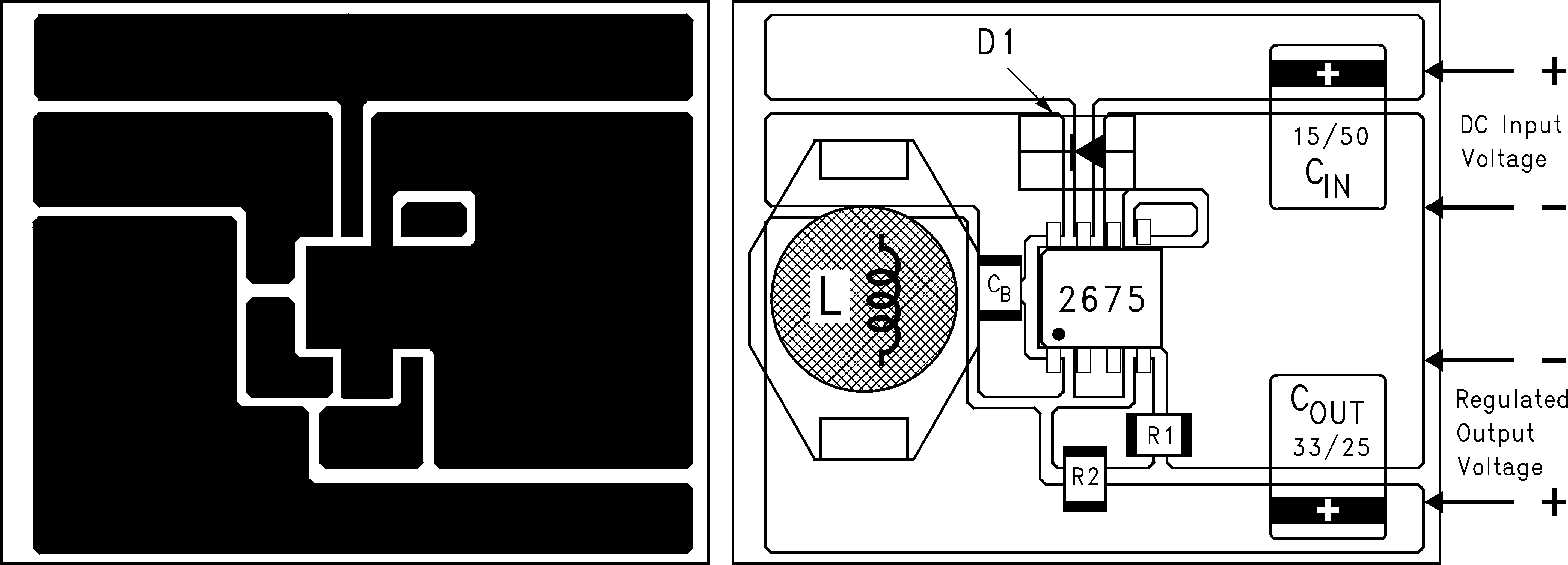
Layout is very important in switching regulator designs. Rapidly switching currents associated with wiring inductance can generate voltage transients which can cause problems. For minimal inductance and ground loops, the wires indicated by heavy lines (in Figure 19 and Figure 24) must be wide printed circuit traces and must be kept as short as possible. For best results, external components must be placed as close to the switcher IC as possible using ground plane construction or single-point grounding.
If open-core inductors are used, take special care as to the location and positioning of this type of inductor. Allowing the inductor flux to intersect sensitive feedback, IC ground path, and COUT wiring can cause problems.
When using the adjustable version, take special care as to the location of the feedback resistors and the associated wiring. Physically locate both resistors near the IC, and route the wiring away from the inductor, especially an open-core type of inductor.
11.1.1 WSON Package Devices
The LM2675 is offered in the 16-pin WSON surface-mount package to allow for increased power dissipation compared to the SOIC and PDIP.
The die attach pad (DAP) can and must be connected to PCB Ground plane or island. For CAD and assembly guidelines see AN-1187 Leadless Leadframe Package (LLP).
11.2 Layout Examples

COUT = 68-μF, 16-V, Solid Tantalum Sprague 594D series
D1 = 1-A, 40-V Schottky Rectifier, surface mount
L1 = 33-μH, L23, Coilcraft DO3316
CB = 0.01-μF, 50-V ceramic

COUT = 33-μF, 25-V, Solid Tantalum Sprague 594D series
D1 = 1-A, 40-V Schottky Rectifier, surface mount
L1 = 68-μH, L30, Coilcraft DO3316
CB = 0.01-μF, 50-V ceramic
R1 = 1k, 1%
R2 = Use formula in Detailed Design Procedure