JAJS611O March 2000 – June 2016 LM2679
PRODUCTION DATA.
- 1 特長
- 2 アプリケーション
- 3 概要
- 4 改訂履歴
- 5 Pin Configuration and Functions
-
6 Specification
- 6.1 Absolute Maximum Ratings
- 6.2 ESD Ratings
- 6.3 Recommended Operating Conditions
- 6.4 Thermal Information
- 6.5 Electrical Characteristics - 3.3 V
- 6.6 Electrical Characteristics - 5 V
- 6.7 Electrical Characteristics - 12 V
- 6.8 Electrical Characteristics - Adjustable
- 6.9 Electrical Characteristics - All Output Voltage Versions
- 6.10 Typical Characteristics
- 7 Detailed Description
- 8 Application and Implementation
- 9 Power Supply Recommendations
- 10Layout
- 11デバイスおよびドキュメントのサポート
- 12メカニカル、パッケージ、および注文情報
パッケージ・オプション
メカニカル・データ(パッケージ|ピン)
サーマルパッド・メカニカル・データ
- KTW|7
発注情報
7 Detailed Description
7.1 Overview
The LM2679 provides all of the active functions required for a step-down (buck) switching regulator. The internal power switch is a DMOS power MOSFET to provide power supply designs with high current capability, up to 5 A, and highly efficient operation.
The LM2679 is part of the SIMPLE SWITCHER® family of power converters. A complete design uses a minimum number of external components, which have been predetermined from a variety of manufacturers. The software is provided free of charge and can be downloaded from Texas Instruments Internet site: www.ti.com.
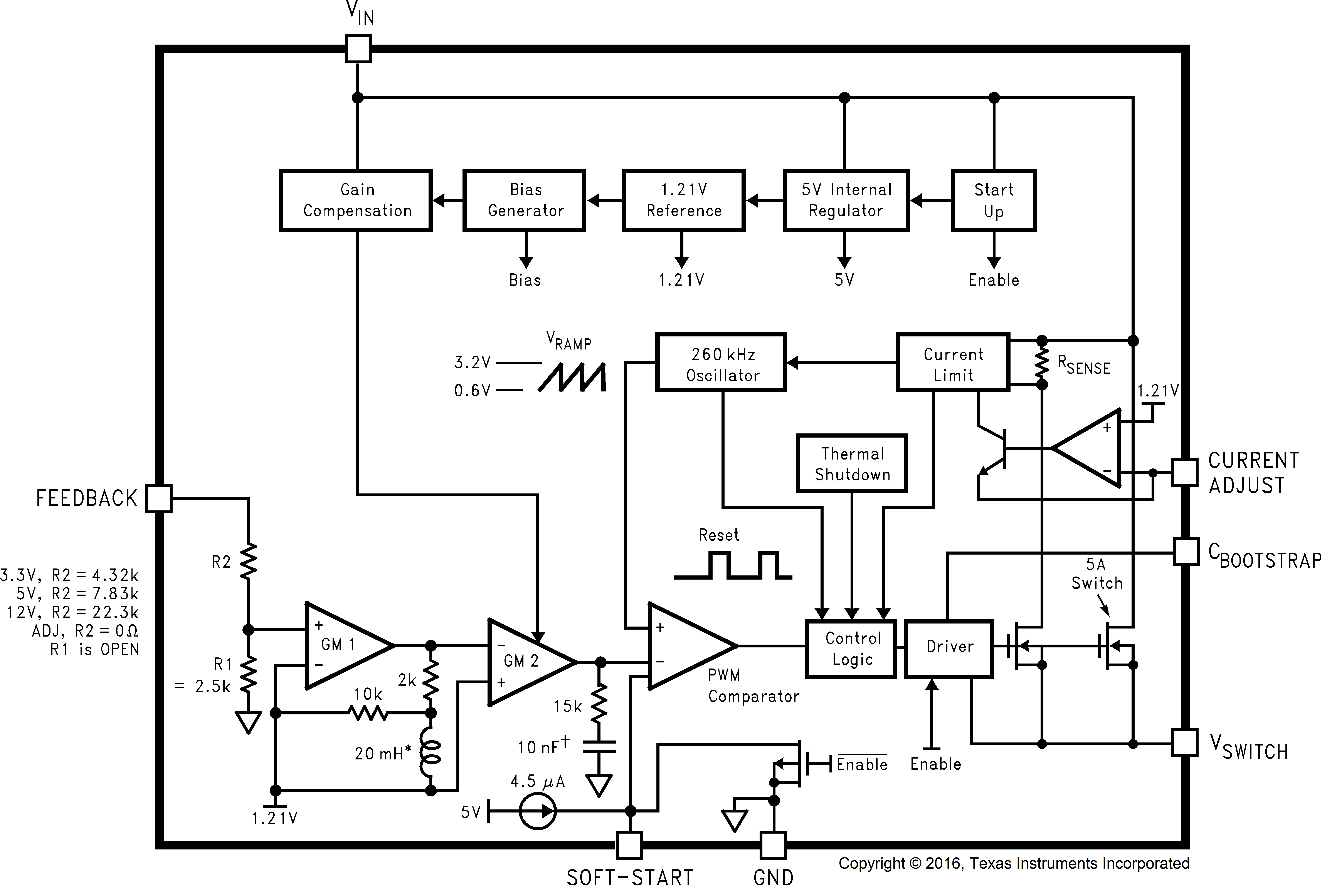
7.2 Functional Block Diagram

7.3 Feature Description
7.3.1 Switch Output
This is the output of a power MOSFET switch connected directly to the input voltage. The switch provides energy to an inductor, an output capacitor and the load circuitry under control of an internal pulse-width-modulator (PWM). The PWM controller is internally clocked by a fixed 260-kHz oscillator. In a standard step-down application the duty cycle (Time ON/Time OFF) of the power switch is proportional to the ratio of the power supply output voltage to the input voltage. The voltage on pin 1 switches between VIN (switch ON) and below ground by the voltage drop of the external Schottky diode (switch OFF).
7.3.2 Input
The input voltage for the power supply is connected to pin 2. In addition to providing energy to the load the input voltage also provides bias for the internal circuitry of the LM2679. For ensured performance the input voltage must be in the range of 8 V to 40 V. For best performance of the power supply the input pin must always be bypassed with an input capacitor placed close to pin 2.
7.3.3 C Boost
A capacitor must be connected from pin 3 to the switch output, pin 1. This capacitor boosts the gate drive to the internal MOSFET above VIN to fully turn it ON. This minimizes conduction losses in the power switch to maintain high efficiency. The recommended value for C Boost is 0.01 μF.
7.3.4 Ground
This is the ground reference connection for all components in the power supply. In fast-switching, high-current applications such as those implemented with the LM2679, TI recommends that a broad ground plane be used to minimize signal coupling throughout the circuit.
7.3.5 Current Adjust
A key feature of the LM2679 is the ability to tailor the peak switch current limit to a level required by a particular application. This alleviates the requirement to use external components that must be physically sized to accommodate current levels (under shorted output conditions for example) that may be much higher than the normal circuit operating current requirements.
A resistor connected from pin 5 to ground establishes a current (I(pin 5) = 1.2 V / RADJ) that sets the peak current through the power switch. The maximum switch current is fixed at a level of 37,125 / RADJ.
7.3.6 Feedback
This is the input to a two-stage high gain amplifier, which drives the PWM controller. It is necessary to connect pin 6 to the actual output of the power supply to set the DC output voltage. For the fixed output devices (3.3-V,
5-V and 12-V outputs), a direct wire connection to the output is all that is required as internal gain setting resistors are provided inside the LM2679. For the adjustable output version two external resistors are required to set the DC output voltage. For stable operation of the power supply it is important to prevent coupling of any inductor flux to the feedback input.
7.4 Device Functional Modes
7.4.1 Soft Start
A capacitor connected from pin 7 to ground allows for a slow turnon of the switching regulator. The capacitor sets a time delay to gradually increase the duty cycle of the internal power switch. This can significantly reduce the amount of surge current required from the input supply during an abrupt application of the input voltage. If soft start is not required this pin must be left open circuited. See Soft-Start Capacitor, CSS for further information regarding soft-start capacitor values.