JAJSA07F November   2002  – October 2016 LM2705

PRODUCTION DATA.  

  1. 特長
  2. アプリケーション
  3. 概要
  4. 改訂履歴
  5. Pin Configuration and Functions
  6. Specifications
    1. 6.1 Absolute Maximum Ratings
    2. 6.2 ESD Ratings
    3. 6.3 Recommended Operating Conditions
    4. 6.4 Thermal Information
    5. 6.5 Electrical Characteristics
    6. 6.6 Typical Characteristics
  7. Detailed Description
    1. 7.1 Overview
    2. 7.2 Functional Block Diagram
    3. 7.3 Feature Description
    4. 7.4 Device Functional Modes
  8. Application and Implementation
    1. 8.1 Application Information
    2. 8.2 Typical Application
      1. 8.2.1 Design Requirements
      2. 8.2.2 Detailed Design Procedure
        1. 8.2.2.1 Inductor Selection - Boost Regulator
        2. 8.2.2.2 Inductor Selection - SEPIC Regulator
        3. 8.2.2.3 Diode Selection
        4. 8.2.2.4 Capacitor Selection
      3. 8.2.3 Application Curves
    3. 8.3 Additional Applications
  9. Power Supply Recommendations
  10. 10Layout
    1. 10.1 Layout Guidelines
    2. 10.2 Layout Example
  11. 11デバイスおよびドキュメントのサポート
    1. 11.1 デバイス・サポート
      1. 11.1.1 Third-Party Products Disclaimer
    2. 11.2 ドキュメントの更新通知を受け取る方法
    3. 11.3 コミュニティ・リソース
    4. 11.4 商標
    5. 11.5 静電気放電に関する注意事項
    6. 11.6 Glossary
  12. 12メカニカル、パッケージ、および注文情報

パッケージ・オプション

メカニカル・データ(パッケージ|ピン)
サーマルパッド・メカニカル・データ
発注情報

Layout

Layout Guidelines

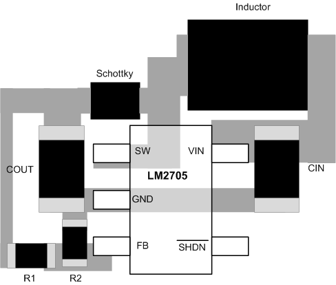
The input bypass capacitor CIN, as shown in Figure 25, must be placed close to the device. This reduces copper trace resistance, which effects input voltage ripple of the LM2705 device. For additional input voltage filtering, a 100-nF bypass capacitor can be placed in parallel with CIN to shunt any high frequency noise to ground. The output capacitor, COUT, must also be placed close to the device. Any copper trace connections for the COUT capacitor can increase the series resistance, which directly effects output voltage ripple. Keep the feedback network, resistors R1 and R2, close to the FB pin to minimize copper trace connections that can inject noise into the system. The ground connection for the feedback resistor network must connect directly to an analog ground plane. Tie the analog ground plane directly to the GND pin. If no analog ground plane is available, the ground connection for the feedback network must tie directly to the GND pin. Minimize trace connections made to the inductor and Schottky diode to reduce power dissipation and increase overall efficiency.

Layout Example

LM2705 layout_snvs191.gif Figure 25. LM2705 Layout Example