JAJSA07F November   2002  – October 2016 LM2705

PRODUCTION DATA.  

  1. 特長
  2. アプリケーション
  3. 概要
  4. 改訂履歴
  5. Pin Configuration and Functions
  6. Specifications
    1. 6.1 Absolute Maximum Ratings
    2. 6.2 ESD Ratings
    3. 6.3 Recommended Operating Conditions
    4. 6.4 Thermal Information
    5. 6.5 Electrical Characteristics
    6. 6.6 Typical Characteristics
  7. Detailed Description
    1. 7.1 Overview
    2. 7.2 Functional Block Diagram
    3. 7.3 Feature Description
    4. 7.4 Device Functional Modes
  8. Application and Implementation
    1. 8.1 Application Information
    2. 8.2 Typical Application
      1. 8.2.1 Design Requirements
      2. 8.2.2 Detailed Design Procedure
        1. 8.2.2.1 Inductor Selection - Boost Regulator
        2. 8.2.2.2 Inductor Selection - SEPIC Regulator
        3. 8.2.2.3 Diode Selection
        4. 8.2.2.4 Capacitor Selection
      3. 8.2.3 Application Curves
    3. 8.3 Additional Applications
  9. Power Supply Recommendations
  10. 10Layout
    1. 10.1 Layout Guidelines
    2. 10.2 Layout Example
  11. 11デバイスおよびドキュメントのサポート
    1. 11.1 デバイス・サポート
      1. 11.1.1 Third-Party Products Disclaimer
    2. 11.2 ドキュメントの更新通知を受け取る方法
    3. 11.3 コミュニティ・リソース
    4. 11.4 商標
    5. 11.5 静電気放電に関する注意事項
    6. 11.6 Glossary
  12. 12メカニカル、パッケージ、および注文情報

パッケージ・オプション

メカニカル・データ(パッケージ|ピン)
サーマルパッド・メカニカル・データ
発注情報

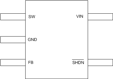
Pin Configuration and Functions

DBV Package
5-Pin SOT-23
Top View
LM2705 20039702.gif

Pin Functions

PIN TYPE DESCRIPTION
NO. NAME
1 SW Input Power switch input. This is the drain of the internal NMOS power switch. Minimize the metal trace area connected to this pin to minimize EMI.
2 GND Ground - tie directly to ground plane.
3 FB Input Output voltage feedback input — set the output voltage by selecting values for R1 and R2 using: R1 = R2 × (VOUT / 1.237 V) –1
4 SHDN Input Active low shutdown - drive this pin to > 1.1 V to enable the device. Drive this pin to < 0.3 V to lace the device in a low-power shutdown.
5 VIN Input Analog and power input supply pin